Table Of Contents
CHAPTER 8
This chapter contains a number of projects by other authors. The only way to understand how to program is to study lots of programs. This includes reading other peoples programs so you can pick up different hints and tricks.
Clicking on the following will take you down the page:
- CHAPTER 8
- FLASHING A LED
- FLICKERING CANDLE
- SWISH STICK
- PIC MINI DICE
- PSEUDO RANDOM NOSE
- QUIZ CONTROLLER FOR 3 PLAYERS
- KEYBOARD WITH 1 WIRE
- PIC10F200 DRIVING 12 LEDS
Note: The instructions in your program should be in small lettering as shown in “Flickering Candle.”
The terms used in the following programs, such as $+2, ds, are covered in the: Library of Routines.
FLASHING A LED
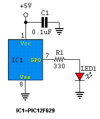
This program flashes a LED. It’s the simplest program you can get.
;
; list directive to define processor
        list      p=12f629
        ; processor specific variable definitions
        #include __CONFIG   _cp_off & _mclre_off & _wdt_off & _intrc_osc_noclkout
                  & _boden_off & _cpd_off &_pwrte_off #DEFINE   LED GPIO,0
    #DEFINE LED_IO  TRISIO,0

CNT0    EQU 20H
CNT1    EQU 21H
CNT2    EQU 22H
;---------------------------------
    ORG 0000H

    MOVLW   07H
    MOVWF   CMCON         ; TURN-OFF analog comparator

    BSF   STATUS,RP0    ; select bank 1
    CALL    3FFH            ; Load cal value
    MOVWF   OSCCAL
    BCF   LED_IO          ; set as output
    BCF   STATUS,RP0    ; select bank 0

LOOP:   BSF   LED
      CALL  DELAY
      BCF       LED
      CALL  DELAY
      GOTO  LOOP

;---------------------------------
; DELAY 0.5 SECONDS ROUTINE
;---------------------------------
DELAY:  MOVLW   03H
        MOVWF   CNT0
        MOVLW   18H
        MOVWF   CNT1
        MOVLW   02H
        MOVWF   CNT2
Delay_0
        DECFSZ  CNT0, f
        GOTO      $+2
        DECFSZ  CNT1, f
        GOTO      $+2
        DECFSZ  CNT2, f
        GOTO      Delay_0

        GOTO      $+1   ;delay 2 cycles
        GOTO      $+1   ;delay 2 cycles
        GOTO      $+1   ;delay 2 cycles
        RETURN ;4 cycles (including call)


    END
FLICKERING CANDLE
This program comes from: http://mondo-technology.com/
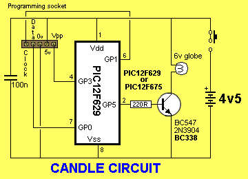
It simulates a candle and is powered by 3 “AAA” cells. The flickering looks so real, all visitors think it is a real candle inside a large jar.
Here is the program:
 ;  Candle Simulation
;   6/04 Luhan Monat
;
;   Simulate flicker of candle using incandescent lamp
    device  PIC12F675,intrc_osc,pwrte_on,wdt_off

    org 20h  ;This is file 20h  - first General Purpose File

del1    ds  1
del2    ds  1
pcnt    ds  1
temp    ds  1
lev1    ds  1
lev2    ds  1
level   ds  1
rbuf    ds  5     ;five files have been allocated

LAMP    =   gp.5

    org 0
    goto    start         ;the program will start at location 0005

    org 4             ;this is the Return From Interrupt location
    reti

start   bsf   RP0     ;the start of the program
      movlw 0
      movwf GP
      movlw 127     ;this is decimal 127
      movwf OSCCAL
      bcf     RP0
      bsf     rbuf,0    ;seed random number
      movlw 127
      movwf lev1      ;initial light level
      movwf lev2


; Main Loop
; Create hi and low power levels
; Switch between levels

candle  movf    lev1,w
        movwf   level
        call    power   ;do lev1 power
        call    rando
        andlw   7
        btfss   z       ;test the zero bit of the working register
        goto    :run    ;skip 7 out of 8
        call    rmid    ;generate new hi and low levels
        movwf   lev1
        sublw   0
        movwf   lev2
:run      movf  lev2,w;do lev2 power
        movwf   level
        call    power
        goto    candle

; PWM power control

power   movlw   100     ;set flicker rate: higher=slower
        movwf   pcnt      ;set loop count
:p1   movf  level,w ;get target level
      movwf del1      ;set 1st delay
      sublw 0         ;
      movwf del2      ;set 2nd delay
      bsf     LAMP    ;power on
:p3   nop
      decfsz    del1    ;do 1st delay
      goto    :p3
      bcf       LAMP    ;power off
:p4   nop
      decfsz    del2    ;second delay
      goto    :p4
      decfsz    pcnt
      goto    :p1

; find sum of 4 random numbers
; skews results around 127

rmid    call    rando
      andlw 3fh
      movwf temp
      call  rando
      andlw 3fh
      addwf temp
      call  rando
      andlw 3fh
      addwf temp
      call  rando
      andlw 3fh
      addwf temp,w
      ret       ;return

; Pseudo Rando Number
; "Chop Suey Machine"

rando   movf    rbuf,w
      addwf rbuf+1,w
      movwf rbuf+1
      addwf rbuf+2,w
      movwf rbuf+2
      addwf rbuf+3,w
      movwf rbuf+3
      addwf rbuf+4,w
      movwf rbuf+4
      bcf     c         ;clear the carry bit of rbuf+4
      rlf     rbuf+4
      btfsc c
      bsf     rbuf+4,0
      movf  rbuf+4,w
      addwf rbuf
      ret

    end
SWISH STICK
The program comes from: http://mondo-technology.com/
The three LEDs are mounted on the end of a ruler and the LEDs produce a pattern when it is waved in the air. The circuit is powered by 3 button cells. The circuit turns off after 20 seconds and the switch needs to be reset to start the effect.

;
;   Swish Stick Program
;   8/04 Luhan Monat


    device  pic12f675,intrc_osc,mclre_on,wdt_off

    org 20h

count   ds  2
sumyel  ds  1
sumgrn  ds  1
sumred  ds  1
del0    ds  1
del1    ds  1
del2    ds  1
prn ds  3

YEL =   gp.2
RED =   gp.1
GRN =   gp.0

    org 0

    goto    start


start   bsf   RP0
      movlw 001000b     ;float mclr?
      movwf gp
      movlw 104
      movwf OSCCAL
      bcf     RP0
      movlw 7
      movwf CMCON         ;no comparators
      movlw 111
      movwf prn
      bsf   GP,3          ;raise mclr?

      clrf  count
      movlw 20
      movwf count+1
:nxt    movlw   1
      call  msecs       ;basic loop timing
      call  pseudo
      bcf     RED
      bcf     YEL
      bcf     GRN
      btfsc prn,0
      bsf     RED
      btfsc PRN,1
      bsf     YEL
      btfsc PRN,2
      bsf     GRN
      decfsz    count
      goto  :nxt
      decfsz    count+1
      goto  :nxt
      bcf     RED
      bcf     GRN
      bcf     YEL
      :hang sleep
        goto    :hang


; pseudo random number generator

pseudo  movf    prn,w
        addwf   prn+1
        movf    prn+1,w
        addwf   prn+2
        bcf   c
        rrf   prn+2
        btfsc   c
        bsf   prn+2,7
        movf    prn+2,w
        addwf   prn
        ret

; milliseconds at 4 MHz

msecs   movwf   del1
:2    movlw 250
        movwf   del0
:3    clrwdt
      decfsz    del0
      goto  :3
      decfsz    del1
      goto  :2
      ret

    end
PIC MINI DICE
by: Rickard Gunée
The program comes from: http://www.rickard.gunee.com/projects
Introduction
This project describes a PIC10F200-based electronic dice. The reason I made this was that I had a small corner left over when ordering a panel with a couple of other PCBs and thought I would rather use the corner for something interesting than leave it unused, so I made a dice project. The PCB is quite small, so it is hard to etch it yourself
Even though this is a very simple project, it requires some surface mount soldering skills, proper tools, and a steady hand as it is built with surface mount components only. But it might be a good start if you have experience with through-hole soldering and want to try surface mount.

The complete project
Hardware
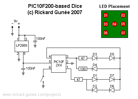
The standard solution for a power supply is to use a 7805 but I could not find any 7805 in a sot-23 or smaller outline so I used an LP2985 that is available in a 5-pin sot-23 with 5v/150mA output. I use a 100nF cap on both input and output side of the regulator to get rid of noise etc. I’m using a standard 9v battery to supply the circuit.
The PIC controlling the dice is a PIC10F20X, but it is also possible to use a PIC10F22X (that is what is sold in my web shop as it is almost the same price so I use the 10F222 to get fewer chips in stock as other projects use the 10F222).
Both are microcontrollers with very small RAM and ROM, 16byte/256words of RAM/ROM but there are versions with up to 24byes/512words.
The 10F22X series also has an ADC but that is not needed in this project. Two of the six pins are used for power supply, there is one reset (or input only) pin and three IO-pins. The switch is connected to the input pin.
The three IO-pins are used to drive a 2x2 matrix configuration of the seven LEDs. Some of the the LEDs are connected in series and lit in three sets of two on opposite sides in series and one single LED in the center. The 2x2 matrix configuration is created with three pins by putting the LEDs in opposite directions so when the common line is “0” some LEDs are lit and when the common is “1” other LEDs are lit. This leads to only two sets of LEDs can be lit at one time, either the LEDs in the corners or the ones in the middle. When scanning at 100Hz between the different LEDs it looks like they are all lit at the same time thanks to the persistence of vision effect.
There are 3 resistors in series with the LEDs as the system runs on 5v and the LEDs have a voltage drop of about 2v each. One nice feature of the PIC10F-series is the current consumption, especially in sleep mode. This removes the need for an on/off switch as the dice only uses 0.4uA in standby, so it can be in standby for many years without using up the battery.
Software
The software is very simple, not very good looking and not very optimized but the 16 bytes of RAM and 256 words of ROM are more than enough so there is no need for optimizations (except for the optimizations that are fun to do). It has a main loop that lights some of the LEDs in one pass and the other LEDs in a second pass. The state engine has four states IDLE, WAIT, ROLL and SHOW.
When in the idle state the PIC is set to sleep state and is woken up on pin change (when the switch is pushed). In the wait state, a roll pattern is shown and a counter is generating a random number based on how long the user pushes the button (not a very good random generator but if the button is pushed longer than the mechanically shortest possible time it is quite ok). In the ROLL state the roll animation is shown for two additional seconds just to make it more exciting. Finally in the SHOW state the result is shown for 3.5sec before going back to IDLE, unless the button is pushed and it starts another roll.
Before “taking on” the PIC10Fxxx” the cost of these chip is higher than the PIC12F629 as the PIC12F629’s are sold in larger quantities and thus the costs are less.
This project is only shown as “an idea.” Using a PIC12F629 will save multiplexing the display and produce a brighter output. Also, using a 9v battery and regulator is very wasteful. The supply can be 3 button cells, with no wasted “excess voltage.”
The dice is built with seven LEDs placed like this:
This is the software for a dice based on PIC10F2XX
;
;*******************************************************************************
;* PIC10F2XX-based mini dice (C) Rickard Gunee 2007
;*******************************************************************************

#include p10f222.inc

    list r = dec

    __config   _cp_off & _wdt_off & _IOFSCS_4MHz & _MCLRE_off

;   udata
;temp0    res   1
;temp1    res   1

VDA0          equ   1
VDA1          equ   2

sndbit      equ 0
lpl         equ 1
rpl         equ 2
scrpart     equ 3
close         equ   4
serve         equ   6
screen      equ 7

temp0         equ   0x10
temp1         equ   0x11
temp2         equ   0x12
digit         equ   0x13
state         equ   0x14
time_l      equ 0x15
time_h      equ 0x16
number      equ 0x17

S_IDLE      equ 0x00
S_WAIT      equ 0x01
S_ROLL      equ 0x02
S_SHOW      equ 0x03


;rst        code     0x00               ;Reset Vector
    movwf   OSCCAL
    goto        Start               ;Jump to Start code


; Table with digits and graphics for roll. Note that order of numbers doesn't matter
; because they are shown randomly so the table has been rolled to make roll table
; and digit table overlap thus saving one byte in the table, a lot of memory left
; so it is just to show off.

digits  andlw   7
    addwf   PCL,F
    retlw   B'1001' ;4
    retlw   B'0001' ;5
    retlw   B'1011' ;6
    retlw   B'0100' ;1
    retlw   B'1000' ;2
    retlw   B'0000' ;3 \\
    retlw   B'0101' ;/
    retlw   B'0110' ;-

; big delay loop to create a delay of about w*3cc

bigdelay        movwf     temp1
bigdelay_l0 movlw     0xFF
                movwf     temp0
bigdelay_l1 decfsz  temp0,F
            goto      bigdelay_l1
            decfsz  temp1,F
            goto      bigdelay_l0
            retlw     0


; Initialize ports etc

Start   movlw   B'1000' ; set leds as outputs and switch as input
      tris    GPIO
      clrf    ADCON0    ; disable ADC on PIC10F22X
      movlw     B'00000000'
      option
      clrf    time_l    ;clear time
      clrf      time_h
main:

;display phase 1
    movfw   digit     ;for a given digit
    call    digits  ;get on/off values for the four LED sets
    movwf   temp2     ;store in temp2 for phase 2
    andlw   B'0011' ;mask out lower 2 bits
    movwf   GPIO      ;output to LEDs (also sets common to low)

    movlw   3
    call    bigdelay    ;wait for 1/200 second


;display phase 2
    rrf     temp2,F     ;shift down upper two bits
    rrf     temp2,W
    xorlw     B'0100'       ;set common line bit to high
    movwf     GPIO        ;output to LEDs

    movlw   3
    call    bigdelay        ;wait for 1/200 second


;handle timer

    incf    time_l,f    ;increase timer low byte
    skpnz               ;if overflow
    incf    time_h,f    ;then increase timer high byte


;handle main state machine

    movfw   state       ;switch on state
    andlw   0x03        ;prevent illegal jump to be safe
    addwf   PCL,F       ;jump to state jump (one of 4 lines below)
    goto    state_idle
    goto    state_wait
    goto    state_roll
                ;"fallthrough" to show state below


;- Show state, shows the result

state_show
      movlw S_WAIT
      btfss GPIO,3      ;if button is pressed
      movwf state         ;set state to WAIT to make another roll
      movfw time_h      ;check if time = 512 main loop cycles
      xorlw 0x2
      skpz
      goto  main        ;if not get back to main and keep waiting
      clrf  state       ;otherwise: set idle state
      clrf  GPIO        ;turn of leds
      sleep             ;go to sleep

;--------------------------------------------------------
; this is the state where the system wakes up
state_idle
      btfsc GPIO,3      ;if button was not pressed
      sleep               ;then power down
      movlw S_WAIT
      movwf state         ;otherwise set state to wait
      goto  main

;--------------------------------------------------------
;- Wait for button to be released and decrease number
;- to get user pressing time to generate a random value

state_wait
      movlw S_ROLL
      btfss GPIO,3      ;if button is released
      goto  state_wait_j0
      movwf state         ;set state to roll
      clrf  time_l      ;and clear time
      clrf  time_h

state_wait_j0
      decfsz    number,F          ;decrease number
      goto    state_wait_j1
      movlw   6               ;restart at 6 if zero
      movwf   number            ;resulting in a "random" number of 0..5
state_wait_j1
        goto    spin                ;show spin effect


;--------------------------------------------------------
;- Roll state, this is just to get some tension, rolling for a couple of extra seconds

state_roll
      movfw time_h
      xorlw 0x1               ;check if time = 256 main loop cycles
      skpz
      goto  spin;               ;if not get show spin effect before getting
                                    ;back to main and keep waiting

      movlw S_SHOW            ;otherwise, set state = show
      movwf state
      clrf  time_l            ;clear time
      clrf  time_h
      decf  number,w            ;set digit to number-1 (result of roll)
      movwf digit
      goto  main                ;go back to main and start showing result


;--------------------------------------------------------
;- Spin effect, shows a rolling sequence of \\/-

spin    movfw   time_l            ;get low part of time
      andlw 0x1F                ;check lower 4 bits
      skpz                      ;if nonzero
      goto  main                ;then continue

        ;the following is done every 16 display cycles

      incf  digit,w           ;else increase digit
      andlw 0x03                ;keep below upper limit
      skpnz                     ;and check for zero
      movlw 0x01                ;additional increase if zero
      xorlw 0x04                ;keep above lower limit
      movwf digit               ;store back to digit
      goto  main                ;get back to main loop

    end
PSEUDO RANDOM NOSE
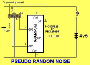
This program produces random noise with an output frequency of approx 50kHz. This is only a “partial program” to show the concept of
The algorithm for generating the noise signal is quite simple. The process begins by setting up a 15 bit shift register, with the initial value of all 15 bits set as 1’s. The register is right shifted, and the lowest bit is transferred to the output register GPO. The lowest and second lowest bits are Exclusive OR’ed, and the result shifted into the highest bit position. The cycle is repeated, with each cycle producing a bit in a pseudo-random bit sequence. The pseudo-random bit sequence repeats each 32,767 cycles.
The output frequency can be decreased by adding delays to the program loop, using an external clock, or using the internal clock/counter/prescaler.

;Pseudo Random Noise
;microprocessor to suit your requirements

HIGH BYTE   equ 007             ; define high byte of shift register
LOW_BYTE    equ 008             ; define low byte of shift register

LOAD_OPTION movlw    0xDF       ; zero bit 5 of option register to
                option              ; disable timer 0 clock source

LOAD TRIS     movlw 0x08          ; define GPIO 0-2, 4 & 5 as outputs
                tris    GPIO          ; 3 as input (or as needed)

INIT REGS       movlw   0xff
            movwf   HIGH BYTE   ;Initialize all bits of registers to 1
            movwf   LOW_BYTE

GEN PRBS      bcf   HIGH BYTE,7   ;set shift-in value to 0
            rrf HIGH BYTE,1   ;shift high byte right
            rrf LOW BYTE,1    ;shift low byte right,
                      ;shift out bit is carry bit in status
            movfw   STATUS      ;load status register
            andlw   0x01          ;isolate carry bit
            movfw   GPIO          ;output new prbs value

GEN SHIFT IN
            xorwf   LOW BYTE,0  ; value for high bit of register
            andlw   0x01          ;isolate shift-in value, sets zero flag if zero
            btfss   STATUS,Z    ;if shift-in bit is zero, skip next
            bsf   HIGH BYTE,6 ;set high bit to 1
            goto    GEN_PRBS

    end
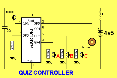
QUIZ CONTROLLER FOR 3 PLAYERS
The Quiz Controller circuit:
;
;***************************************
; written by: John Morton
; for PIC12F675
; clock frequency: Int. 4 MHz
; ***************************************

; Program Description: Quiz controller for 3 players, including reset button
;  for the quiz master

    list        P=12F675
    include     inc:\\pic\\p12f675.inc

;==============
; Declarations:

temp    equ 20h
Post16  equ 21h

    org 0   ; first instruction to be executed
    goto    Start   ;

    org 4   ; interrupt service routine
    goto    isr ;

;===========
; Subroutines:

Init    bsf   STATUS, RP0   ; go to Bank 1
      call  3FFh            ; call calibration address
      movwf OSCCAL        ; move w. reg into OSCCAL

      movlw b'011110'       ; GP5: Buzzer, GP3: Reset button
      movwf TRISIO        ;  GP1,2,4: LEDs/Buttons (inputs
                ;  to start with), GP0: LED enable
      movlw b'010110'       ; GP1,2,4 have weak pull-ups
      movwf WPU           ;   enabled

      movlw b'00000111' ; pull-ups enabled, TMR0 presc.
      movwf OPTION_REG  ;  by maximum (256)
      clrf  PIE1            ; turn off peripheral interrupts
      movlw b'010110'       ; enable GPIO change interrupt
      movwf IOC           ;  on GP1, GP2 and GP4 only
      clrf  VRCON           ; turn off comparator V. ref.
      clrf  ANSEL           ; make GP0:3 digital I/O pins

      bcf     STATUS, RP0   ; back to Bank 0
      clrf  GPIO            ; reset input/output port
      movlw b'00001000' ; enable GPIO change interrupt
      movwf INTCON        ;  only
      movlw b'00000111' ; turn off comparator
      movwf CMCON           ;
      clrf  T1CON           ; turn off TMR1
      clrf  ADCON0        ; turn off A to D converter

      movlw d'16'           ; set up postscaler
      movwf Post16        ;
      retfie                  ; return, enabling interrupts

;====================
; Interrupt Service Routine
isr btfss   INTCON, 0         ; check GPIO change int. flag
          goto  Timer         ; TMR0 interrupt occurred?
                ; GPIO interrupt occurred?
        bcf INTCON, 0       ; reset interrupt flag
        comf    GPIO, w     ; store state of GPIO
        andlw   b'010110'   ; mask all except buttons
        movwf   temp            ;
        btfsc   STATUS, Z   ; are any buttons actually pressed?
        retfie              ; false alarm
        bsf STATUS, RP0 ; to Bank 1
        movlw   b'001000'   ; make GP1,2,4 outputs
        movwf   TRISIO      ;
        bcf STATUS, RP0 ; move to Bank 0
        movfw   temp          ; move temp back into GPIO,
        addlw   b'100001'   ;  set GP5 and GP0 (turns on
        movwf   GPIO          ;  buzzer and enables LEDs)
        movlw   b'00100000' ; enable TMR0 interrupt, disables
        movwf   INTCON      ;  the GPIO change interrupt
        retfie              ; return, enabling GIE

Timer   bcf     INTCON, 2   ; reset TMR0 interrupt flag
      decfsz    Post16, f   ; is this the 16th TMR0 interrupt
      retfie                  ;

      bcf   GPIO, 5         ; turn off buzzer
      clrf  INTCON        ; turn off all interrupts
      sleep                 ; go into low power mode

;============
; Program Start

Start   call    Init            ; initialisation routine

Loop    goto    Loop            ; keep looping

        END
KEYBOARD WITH 1 WIRE
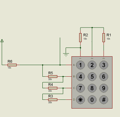
The following circuit shows how to connect resistors to a keyboard for a 1-wire communication to a micro. The line is taken to the ADC of the micro. When a key is pressed it produces a unique resistance and this is interpreted by a sub-routine.
PIC10F200 DRIVING 12 LEDS
The interesting feature of this circuit is the function of the two transistors. They are designed to reduce the voltage of the power supply so that the LEDs do not illuminate when one or more of the output lines are made “input.”
Suppose all drive lines are made input.
You can see a red LED and orange LED are connected directly across the power rails in two of the branches. These LEDs would illuminate if the supply was higher than 1.7v + 2.3v = 4v.
The two transistors are designed to drop the rail voltage.
To work out the rail voltage we note the 3k3, 2k7 and 2k2 are voltage dividers. The voltage across the 3k3 will be 5 / 8.2 x 3.3 = 2v
The voltage on the base of the BC182 will be 5v - 2.6v = 2.4v
This means the supply voltage for the LEDs will be 2.4v This means any output taken LOW will deliver slightly less than 2.4v for any LED connected between the drive-line and Vref1.
The BC 213 drops 5 / 8.2 x 2.2 = 1.3v
A drive line supplying voltage to the orange and green LEDs will have slightly less than 3.7v available.
The different base resistor shave been chosen to produce approx the same current though each of the LEDs.
The chip can only drive some of the LEDs at the same time and this is covered in some of our other articles.

Tags
Quick Links
Legal Stuff
Social Media


