Table Of Contents

3-TRANSISTOR CIRCUITS
Three transistors will give a wide range of designs. Here are 6 circuits showing how to connect a buffer stage to an oscillator.
But first we need to show the buffer can be connected to the oscillator stage via point A or point B.
Point A has a higher amplitude but since this point is a high-impedance point, any energy taken from this point will affect the amplitude of the oscillator. Point B a low-impedance point, but has a much lower amplitude
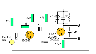
Connecting a buffer to point A or point B
Thus we have a decision to make. I prefer the collector take-off point as it has a larger signal and this signal can be passed to the buffer stage via a small capacitor to fully drive the buffer transistor.
The capacitor will actually convert a large signal with low current into a smaller signal with higher current. This is one of amazing things a capacitor will do.
You may think point A is a low impedance point as it is just a fraction of an ohm away from the positive rail. But the inductor (coil) is creating a voltage and waveform at point A and if any load is applied at this point, the waveform will decrease, because the inductor does not have much “strength” to produce the waveform. It does not have much strength because the transistor is being driven very lightly and the stage is only consuming very little current.
To understand this more clearly, you need to know how the stage works so you can see how delicate the circuit is.
When the power is applied, the circuit starts to operate due to the 47k bias resistor on the base.
The next point to note is the base is held rigid by the 1n on the base. This capacitor has an impedance of less than one ohm at 100MHz and you can consider the 1n as a 2v battery with an impedance of 1 ohm or a one ohm resistor sitting on top of a 2v battery. In any case the base is held very rigid by the 1n.
Now we come to understanding how an NPN transistor “turns on.”
It can be turned on in two ways. The emitter can be held rigid and the base can be raised to 0.6v and if the voltage is raised slightly more and the base is fed with current, the transistor will conduct and current will flow in the collector-emitter circuit.
This is the case with the transistor in the audio stage. The emitter is held rigid and the base is fed with current, once the base is above 0.65v.
The other way to turn on an NPN transistor is to hold the base firm and lower the emitter. Once the emitter is lower than the base by 0.65v, the transistor turns on and if the emitter is lowered slightly more, the transistor turns on more.
This may be difficult to visualise, but this is occurring in the oscillator stage.
Let’s advance a few cycles and see what is happening.
The transistor turns on and the collector pushes the top of the 10p capacitor towards the emitter.
The energy in the capacitor gets converted to a small voltage and larger current. We said before, that a capacitor can do this.
The small voltage pushes the emitter lower and this turns ON the transistor. The result is a little bit of energy is pumped into the capacitor in the tuned circuit.
At this instant, the coil does not get energy from the transistor because a coil resists any quick flow of current into it and it acts like a very large resistor.
The energy in the 10p is now spent and the transistor turns off slightly. The energy from the capacitor in the tuned circuit passes to the coil and when the capacitor can no-longer keep the flux in the coil increasing, there comes a point where the flux starts to collapse. This flux produces a voltage that is larger than before and is opposite to the previous voltage.
This is one of the amazing things of a coil and capacitor in parallel. The voltage at the lower end of the coil-capacitor combination is higher than the supply and this raises the top plate of the 10p capacitor. This rises the voltage on the emitter and turns the transistor off completely.
This allows the tank circuit to produce its amazing HIGH VOLTAGE without the transistor loading the circuit.
But he coil/capacitor is a very delicate arrangement and it is producing the high voltage at very low current as it is converting the original low voltage small current into high voltage very low current.
If we put a load on the circuit at point “A” we will reduce the voltage and may freeze the circuit.
The following 9 circuits show different ways to “tap-off” the waveform and amplify it in a stage called a BUFFER.
The BUFFER converts a HIGH IMPEDANCE signal into a LOW IMPEDANCE signal as the antenna is commonly referred to as a 50 OHM LOAD.
The simplest buffer is shown in the following circuit. It is a common emitter stage with a resistive load.
1. STABILITY
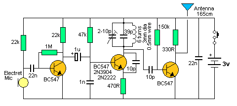
BC547 is not suitable as a buffer
A BC 547 transistor is not very good at amplifying at 100MHz. The circuit above does not give a range greater than the 2-transistor version, but the stability is much greater. The antenna can be touched without the bug drifting off frequency.
2. INCREASED RANGE
To increase the range, the output must be increased. This can be done by using an RF transistor and adding an inductor. This effectively converts more of the current taken by the circuit into RF output. The output is classified as an untuned circuit.

Use an RF transistor for the Buffer
3. MORE RANGE
More output can be obtained by increasing the voltage and adding a capacitor to the output to tune the buffer stage. The 5-30p must be adjusted each time the frequency of the bug is changed. This is best done with a field strength meter. See Talking Electronics Field Strength Meter project.
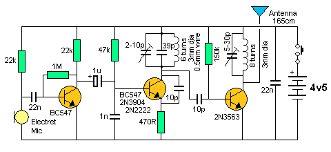
A tuned output stage delivers more output
The 2N3563 is capable of passing 15mA in the buffer stage and about 30% is delivered as RF. This makes the transmitter capable of delivering about 22mW.
The 2N3563 is also available as PN2563 where PN signifies “plastic package.”
These (this) transistor is not a POWER TRANSISTOR. It is classified as a SMALL-SIGNAL TRANSISTOR and even though the .pdf indicates the collector current is 50mA, you will notice all the specifications are provided at 8mA! That’s why we have allowed a maximum current of 15mA for our calculations.
2N3563.pdf
The 2N3563 (PN3563) is readily available at electronics stockists (Talking Electronics sells them for 90cents for two).
ULTIMA FM BUG - 1km TRANSMITTER
This circuit is available from Talking Electronics as a kit. See the full article HERE.
It has a range of 1km using a 6v supply. The article shows how to peak the project using a LED Power Meter.
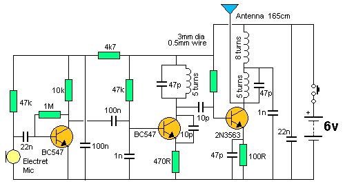
Ultima FM Transmitter
4. DIFFERENT COUPLING
We have already mentioned the fact that a capacitor can convert a large waveform with low current into a small waveform with large current.
The following circuit taps off the inductor at a point of low amplitude to put the least load on the tank circuit. The coupling capacitor has been increased to transfer enough energy at low amplitude.
This coupling has exactly the same result as shown in circuit 3.
Circuit 3 is preferred as it is easier to connect to the collector than tap the inductor.

Tapping the oscillator tuned circuit
5. A PNP BUFFER
A PNP transistor can be used in the buffer stage, but as we said before the BC557 is not as good as an NPN transistor, when operating at high frequencies.

A PNP in the buffer is not a good performer

A PNP in the buffer is directly connected
The circuit above shows a PNP transistor (buffer) connected directly to the oscillator. The buffer is turned ON during part of the cycle when the oscillator transistor is turning ON and the voltage developed across the top 3 turns of the coil is greater than 0.65v.
This design puts a heavy load on the tank circuit and you will see the previous design has a base resistor to provide this function.
In addition, the 39p emitter bypass capacitor is not needed.
6. WASTED POWER
The following circuit (from the web) takes 30mA. This is wasted current. As we said before, any voltage above 4.5v is excess and any current above 12mA for this type of circuit is excess. A BC 557 cannot deal with any more than 5mA collector-emitter current. Any more than 5mA is wasted. That’s why you need an RF transistor in the output.

The buffer is taking excess current
##7. EMITTER TAP The following circuit taps the emitter of the oscillator stage. We have already explained the collector or the emitter can be tapped and produce about the same results.
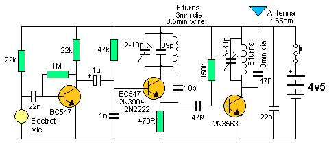
Tapping the emitter of the oscillator transistor
8. CLASS “C” OUTPUT
The following circuit uses no biasing on the output transistor. It gets all the energy to activate the base from the oscillator stage.
While this is possible, the amount of energy needed is very large and the oscillator cannot provide enough energy to fully drive the output stage. For the cost of a fraction of a milliamp, it is better to bias the output transistor and get a much-greater output.
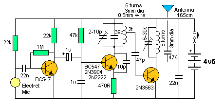
Class “C” output
9. ADJUSTABLE OSCILLATOR COIL
To make a circuit more compact or cheaper (of if you don’t have a trimmer), the oscillator coil can be adjusted by stretching or compressing. When the coil is stretched, the frequency increases. The buffer circuit has to be adjusted too, to get the greatest output.

Adjustable oscillator coil (no trimmer capacitor)
10. POOR DESIGN
Here is a circuit with poor design. It goes against 6 of the things we have mentioned above.
The first poor design is the low value resistance for the microphone. For 9v, the microphone load resistor should be 47k. If a low value is used, the microphone will will over-amplify and create a background noise similar to bacon and eggs frying.
The 100k separating the microphone from the base of the audio transistor is not needed. If the microphone is operated at its correct level of current, this resistor will not be needed.
The BC 547 is self biased via the 1k and 100k, so the 22k resistor on the base is not needed.
The 100R on the emitter of the BC338 is a very low value for 9v supply.
The coil is on the PC board has a very low “Q” and the current taken by the circuit is excessive when the emitter resistor is 100R.
The 22p in series with 2-30p gives a value about 2p to 12p and this is very small for this tank circuit.
Series capacitors make it very difficult to adjust the frequency as the trimmer is having a lot of effect on changing the frequency when it is in series with another capacitor.
The final unusual feature is the 10u and 100u electrolytics. We have already mentioned that electrolytics do not have any effect with frequencies around 100MHz. It seems the designer had difficulties with audio instability, due to the low value of resistance on the microphone and tried to fix the problem with electrolytics. The circuit has 4 unnecessary components and if you are going into manufacturing, these will be a costly mistake.
This project is to be avoided if you want a good range with low current consumption. Some of our other circuits are a better choice. The photo below shows the assembled circuit.
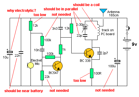
9 wrong things with a circuit
There are actually 10 wrong things. The transistor, capacitor and coil are too far from each other. This produces a very poor “Q.”

A photo of the circuit above. This circuit is a very poor design. It was produced by a non-technician. That’s why you have to study electronics, so you don’t make a fool of yourself.
11. MORE POOR DESIGNS
Here is another circuit with extra complexity and a useless output stage.

Emitter Injection of output stage
There is no evidence of the above circuit delivering more output than connecting to the oscillator stage. The circuit uses extra components and winding the transformer costs more for no extra benefit. The emitter circuit is very low impedance and the transformer is expected to do a lot of conversion - called impedance matching. It it trying to match 5k to 500R.
The output transistor is in common-base configuration and it is usually used to match impedances or convert the signal from a low impedance device to a circuit with a high impedance input. This is not the requirement in our case. We need a circuit to match a high impedance to a low impedance.
Let’s go over the operation of a common-base stage and show how unsuitable it is in this application.
The emitter is connected to 0v via a 2-turn winding. The base is at approx 0.65v as it cannot rise higher than the emitter, even though the two voltage divider resistors are trying to put 1.5v on the base. And it is held rigid at this voltage via the 1n capacitor, as far as the 100MHz signal is concerned.
When a current flows in the 2-turn winding, a voltage is developed and suppose this voltage is negative. This will drive the emitter lead below the 0v line and actually turn the transistor on more.
This will cause more current to flow in the collector circuit and this current must also flow in the emitter circuit.
This will cause a positive voltage to appear across the 2 turn winding and counteract the effect we have just produced.
In other words, the stage is working against us and making it very difficult to deliver energy to the stage.
The output stage is not adding to the power of the project and it is of no benefit at all. I am surprise it has been presented in electronics manuals as a good design.
12. ANOTHER POOR DESIGN
This project is very well presented on the web, with large, clear photos, but the actual design has a number of poor features.
Here is the circuit diagram:
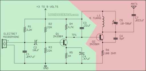
The faults are as follows:
- The 2k2 resistor to the microphone is too low. It should be at least 10k for 3v and 47k for 9v.
- The .047 across the microphone serves no purpose.
- The 10u coupling the microphone to the first transistor can be much smaller, 22n to 100n.
- The direct coupling of the audio stage to RF stage will decrease the frequency stability.
- There is no capacitor across the battery.
When you fix these faults you will see how much improvement you get. It will be considerable.
Here are the photos of the completed transmitter and a very small version:
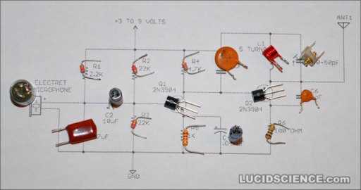
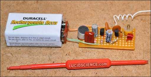

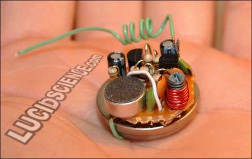
This covers all the possible combinations for the greatest output with three transistors using a 3v to 9v supply.
If you want to improve any of the circuits we have covered, here are some helpful tips:
13. THIS DOESN’T WORK
Some things that look theoretically possible, do not work in practice.
It seems obvious, to increase the power output from a transmitter, simply put two transistors in parallel on the output.
Unfortunately this does not work. The output does not increase. In addition, decreasing the emitter resistor or increasing the biasing does not produce a higher output.
A transistor has a set of parameters and certain capabilities. These have been provide for a reason. They are the maximum you will get from the device.
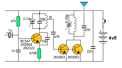
Transistors in parallel does not produce a higher output
14. A GOOD CIRCUIT

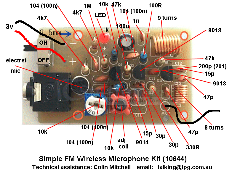
The oscillator in this project uses a SERIES TUNED CIRCUIT circuit made up of an adjustable slug-tuned coil and 15p capacitor. The circuit works very well and the cost of the project is very small from the supplier shown below the circuit.
Only a few points to note: The kit of parts does not include a battery holder or antenna wire or solder. The PCB is possibly nickel plated and not solder-tinned and it is slow to make each solder-connection. The lands are very small and you need a very fine tipped soldering iron to complete the assembly.
3v is the best supply voltage as a higher voltage will overload the oscillator transistor and cause spurious transmission on different parts of the band and may interfere with other stations.
The effectiveness of the “pi” filter on the output to match the impedance of the antenna to the output transistor is very debatable.
The two 47p capacitors should be adjustable because, when you adjust them, the energy delivered to the antenna increases enormously.
In addition, the coupling capacitor is only 15p and this is the major limitation of the amount of energy reaching the antenna.
Compare the 15p with the 200p coupling the oscillator to the buffer transistor. The 200p is only 10 ohms and when you consider the base of the buffer transistor is very low in the way of “resistance,” the 200p should be more like 47p.
The circuit is a Colpitts oscillator because it uses and un-tapped coil.
The circuit starts by the 47k delivering current to the base of the transistor. The top 30p charges (and the 15p charges) and when the base is 0.6v higher than the emitter, the transistor starts to turn ON. Current flows through the 330R and a voltage is produced across this resistor.
The two capacitors keep charging and the transistor turns on more and more. It come to a point where the current supplied by the 47k will not turn the transistor on any harder.
Normally the transistor would stay in this condition but the 15p and coil form a circuit called a SERIES TUNED CIRCUIT.
But it is what happens with the TUNED CIRCUIT that creates the second half of the cycle.
The tuned circuit has been given a pulse of energy and the capacitor has charged because the inductor has produced a back-voltage during this time (called the charging current) and this has produced magnetic flux that cuts all the turns of the coil and produced a back-voltage that only allows a very small current to flow through the coil. The result is the voltage appearing across the two components will mainly appear across the capacitor.
We now come to a point where the voltage on the base is as high as it will get and the 15p is charged to a potential that will not increase. This means the charging current through the 15p will decrease and the magnetic flux from the coil will start to collapse. As it collapses, it produces a voltage in the turns that is of opposite potential and this pulls the 15p down towards the 0v rail. This reduces the voltage on the base and the transistor starts to turn OFF. This action continues until all the magnetic flux is converted to voltage.
The 15p cannot pull the base any lower and it is always fighting against the 47k.
A point comes when the current from the 47k starts to make the base rise again. The competes the two halves of the cycle.
It is the time taken for the inductor to lose its energy that determines the duration of the cycle. The 15p also has an effect on the timing.
Some of the magnetic flux is absorbed by the ferrite core and this changes the timing and thus the frequency at which the circuit operates.
HOW A CAPACITOR WORKS
It’s handy to know the effective reactance (resistance) of a capacitor at the operating frequency of the circuit. If we assume 100MHz, the resistance is as follows:
| Capacitance | reactance @100MHz | reactance @2kHz |
|---|---|---|
| 5.6p | 300R | |
| 10p | 166R | |
| 22p | 75R | |
| 47p | 35R | |
| 1n | 1R6 | |
| 22n | much less than 1R | 3k7 |
| 1u | ----- | 82R |
How a capacitor works depends on where it is placed. A 22n across the power rails will be like a small battery equal to the voltage of the supply, but with an internal resistance of less than one ohm.
When a battery has a low internal impedance, a high current can be taken without the voltage dropping. You may not think the oscillator circuit takes a high current but if the average is 10mA, there will be times when the circuit requires 20mA, and times when it needs 1mA.
If the voltage dips when the circuit is trying to charge a capacitor, for example, the capacitor will not get charged to its maximum.
This is what happens with the circuits above. As soon as you put a 22n across the battery, the output increase a small amount.
Not only does the output increase, but the increase stays throughout the life of the battery, especially when it is getting flat. So the 22n across the battery is very important.
A ceramic capacitor is able to supply this tiny amount of charge very quickly and this is needed as the circuit is working at 100,000,000 times per second.
An electrolytic is not able to supply a tiny amount of charge at this fast rate and so an electrolytic is not suitable for the supply “decoupler.”
A decoupler is the name given to any capacitor that is placed across the supply rails to suppress spikes or prevent the effects of one stage from interfering with another stage. It “decouples” or “separates.”
When a capacitor is used to “couple” one stage to the next, such as the 22n between the microphone and base of the audio amplifier, the capacitor has a certain resistance at the frequency of the signal and since this is audio, it has an effective resistance of about 4k. If you put a 4k resistor in place of the 22n, you can see any signal produced by the microphone is only a few kilo ohms away from the base of the audio transistor. The audio transistor has an input impedance of about 4k and thus the two resistances can be seen as joined together in series with the input of the transistor at their middle. They form a voltage divider in which 50% of the signal produced by the microphone is delivered to the transistor.
This is a very simple way to see the situation, so that if the 22n is replaced by a 1n, very little of the signal produced by the microphone will be delivered to the transistor.
But if the 22n is replaced by a 1u, abut 95% of the signal will be delivered.
That’s a choice you have to make. Experiment with the two values and see if the improvement is noticeable.
When a capacitor is used to stabilize a voltage in a building block, such as the 1n on the base of the oscillator, it is acting just like the 22n across the supply and it appears as tiny battery with a voltage of about 2v and a resistance of about 2 ohms. This type of battery will deliver 1 amp, so you can see the 1n will keep the base very stable.
The 10p to 47p coupling the oscillator to the output stage, is equivalent to a very low resistor so nearly all the energy of the oscillator is being passed to the output stage.
This is only a very simple way to look at the operation of each capacitor but it gives an idea of why each value has been chosen.
It’s a pity the designer of circuit #10 did not read these notes before trying to design a kit for the electronics market.
GOING FURTHER
The next stage to improve the output, matches the impedance of the output stage to the impedance of the antenna.
The impedance of the output stage is about 1k to 5k, and the impedance of the antenna is about 50 ohms.
This creates an enormous matching problem but one effective way is with an RF transformer.
An RF transformer is simply a transformer that operates at high frequency. It can be air cored or ferrite cored. The type of ferrite needed for 100MHz is F28. The following circuit uses a small ferrite slug 2.6mm dia x 6mm long, F28 material.
A slug is the screwed rod that screws into a coil and is adjusted to change the matching of the windings or the frequency of the coil or transformer.
To create an output transformer for circuit 6 above, wind 14 turns onto the slug and 4 turns over the 14 turns. The ferrite core will do two things. Firstly it provides a high amount of energy to pass from the primary winding to the antenna. And secondly it will prevent harmonics passing to the antenna.
The only way to prove the effectiveness of the transformer is with a field test and the range increased nearly 100%, over the tuned output design in circuit 9.

Matching the output to the antenna via a transformer

The output transformer
The photo above shows the 14 turns wound on the ferrite slug and 4 turns wound over this winding. Remove the enamel from the 4 ends and solder the leads as shown on the circuit diagram. It does not matter which way the winding is wound and you can experiment with adding more turns to the primary or removing turns from the secondary to get the highest output.
A slight improvement to the design is to make an auto-transformer. The circuit likes the fact that some of the current and voltage is already flowing in the “secondary” of the auto-transformer and it simply adds to this.
The other improvement is to make the output transistor self-biasing by including an emitter resistor. This allows all the transistors in a batch to take approximately the same current as the gain of each transistor will determine the quiescent current, with high-gain devices taking more current.
The addition of the 100R will reduce the spread in quiescent current.
The output of the stage will not fall since the impedance of the 1n at 100MHz is very small.
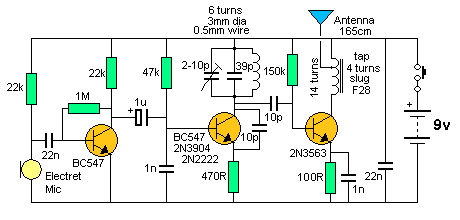
Using an Auto-transformer and self-biasing the output transistor
A transformer is the best way to couple the output of the transmitter to the antenna but capacitors and inductors in an arrangement known as “pi,” “T,” or “L” coupling can be used. This is when you take advantage of the fact that a capacitor can convert a high-voltage at low-current into a low-voltage at high-current and an inductor has a higher impedance at high frequency. It will reduce harmonics and the capacitor will provide a higher current to produce higher electromagnetic radiation. This is how a high impedance (resistance) is converted into a low impedance.
This type of coupling has been added to the following circuit.
This is actually highly effective but the components must be adjusted accurately to have the greatest effect.
In addition, the frequency of the oscillator cannot be changed without having to re-align the output.

The following circuit uses three parallel tuned circuits to couple the output of the transmitter to the antenna.
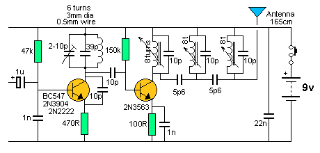
A triple-tuned output stage
Don’t forget, you are trying to connect a 4k impedance of the circuit to a 50 ohm load.
The first tuned circuit is in the collector of the output transistor. It is very similar to the “inductor” circuit above except the capacitor across the coil will improve the performance of the circuit enormously when the slug in the coil is adjusted.
But this arrangement has a disadvantage. The output will only perform to its best on a particular frequency (via the 10p capacitor and 8t coil) when the slug in the coil is turned to produce a maximum output.
The 2-10p air trimmer in the oscillator stage cannot be adjusted without re-tuning the output stage and this limits the versatility of the circuit.
However considerably more energy will be delivered to the antenna when the 3 tuned output stages are adjusted for maximum output. The signal from the first is tapped off with a 5p6 capacitor to the second “TUNED SECTION.” This is the coil and capacitor in parallel.
The second “tuned section” is then adjusted to give maximum output. The energy is then “tapped off” to a third tuned stage to which the antenna is connected.
If you are prepared to have a fixed-frequency circuit, this arrangement is excellent.
It does three things:
- It separates the output stage from the antenna, You can touch the antenna without affecting the frequency.
- It converts more of the energy at the output stage, than previous circuits, and
- It matches the 4k of the output stage to the 50 ohm impedance of the antenna.
Of course there is a lot of very complex mathematics that can be applied to working out the
value if the components needed to interface between the output stage of a circuit and the antenna. But nowhere will you find the “reason” why the components convert the signal from one impedance to another.
For the first time we have told you: “it’s the squeezing action of the capacitor, converting a high-voltage, low-current into a low-voltage high-current.”
This produces the effect of converting a high impedance into a low impedance.
An inductor can convert a low-voltage high-current into a high-voltage, low-current by the collapsing magnetic field producing a very high voltage and this is how we convert a low impedance into a high impedance. You can read more about this in our project: Solar Garden Light.
I am not going to argue with the pure mathematicians about this. I want you to “see” how a circuit works so you can design anything and fix it without having to get out a pencil and paper.
“All that matters in this world is to get something done, get paid, and get on with the next thing.” Leave the arguments ‘till later.
THE COIL
Whenever you see a coil in a circuit, magic things can happen.
This is due to the phenomena of the coil producing a higher voltage (in the opposite direction) when the applied voltage suddenly stops.
And when you see two windings (or one winding with an auto-transformer), you do not know what output you will get without knowing all the details of the transformer and actually seeing it in action.
The most effective oscillator coil has the dimensions of being at least twice as long as its diameter.
In the following photo, the small coil is the TANK COIL and the larger coil (called an inductor) is on the output.
The diameter of the small coil is too large. It has been wound on a 5mm drill. It should be wound on a 3.5mm drill and the number of turns increased from 4 to 6. (The turns are counted at the top of the coil.)
This will improve the “Q” of the coil. The inductor can also be reduced in diameter.
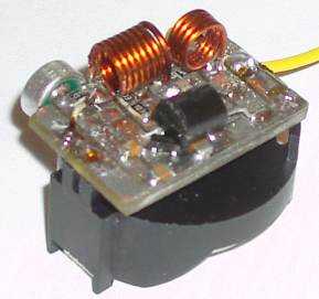
The diameter of the 4-turn TANK COIL is too large
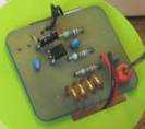
The turns are spaced too wide
The second image shows a 4-turn coil with the turns spaced too wide. The maximum spacing is the thickness of the wire. When the turns are spaced very wide, the “Q” of the coil is reduced and the performance of the circuit reduces.
When the length to diameter is 2:1, it allows the maximum amount of magnetic flux surrounding the coil to collapse back and cut the turns of the coil.
When designing a coil, here are the four most important features:
- The most important feature is getting the length-to-diameter to be at least 2:1
- The next improvement is choosing the core material. Air has a value of 1 at all frequencies. Ferrite (F29 material) will have a value of about 3 at 100MHz. This means the number of turns can be reduced to achieve the same inductance, and the coil will be less prone to external influences such as metal objects, but we have not found the output to be any better than an air coil (in any of the FM transmitters we have designed).
- The next critical factor is the spacing of the turns. The best is close-spaced but they can have a small gap (the width of the wire) and the coil will still be effective.
- The gauge of the wire is not particularly critical however wire thinner than 0.25mm will vibrate and produce microphonic sounds. 0.5mm wire is the maximum you need. Thicker than 0.5mm is not needed.
0.1uH COIL
On some circuits you will find a value of 0.1uH (100nH) for the coil. If you buy a ready-made inductor of this value, the circuit may work or it may not. The reason is the coil in the TANK circuit must have a high value of “Q” to get the greatest range. To achieve a high Q, the coil should be hand-wound as shown in the notes for the circuits. A ready-made inductor will be many turns of very fine wire and will not be in the ratio mentioned above. The wire will also be too fine. In. In addition, a hand-made coil can be adjusted by stretching the turns.
THE ANTENNA
The secret to getting a good range with low power is providing a good transmitting antenna.
In addition, a good ground-plane is also needed. The batteries are normally used to provide a ground-plane and that’s why the leads to the battery must be kept as short as possible. 5cm of battery lead can reduce the output to half. Connecting the battery directly to the board can double the output. Adding a thick ground-plane to the PC board can also help considerably.
But, of course, it is the antenna that does most of the work.
Since we are transmitting at about 100MHz, the wavelength of the signal is 3.3 metres and a full wave antenna would be 3.3 metres long.
It is often quite inconvenient to use a long antenna, so here are some alternatives.
Obviously you can use a shorter antenna, but as you reduce the length, the range reduces.
Surprisingly, it does not decrease greatly when the antenna is reduced to “half-wave” and this is what we have supplied with all Taking Electronics FM transmitters.
Many of the kits on the web are supplied with an antenna 30cm long to reduce the range and make the transmitter somewhat legal. But this is not what building and testing is all about.
The hobbyist wants to know how far he can reach with the transmitter he has made.
Placing the antenna on top of a cupboard is a good choice. It provides height and you can stretch the antenna to its full 1.65m length.
The receiving antenna on a radio must also be horizontal and somewhere at the front or back of the transmitting antenna.
If you require omni directional radiation, (radiation 360°) the antenna must be upright (vertical). The receiving antenna must also be vertical and can be anywhere in the 360° radius.
We are not going into the complexities of different radiating patterns of antennas but here is one suggestion for an improved antenna. It is called a DIPOLE. You can get a closed dipole, folded dipole and others but ours is a simple design.
THE DIPOLE
If you want to transmit in a particular direction, you can fit a dipole antenna..
This is simply connecting one wire to the antenna output and another wire to the 0v rail and stretching each out horizontally in the opposite directions.
These are called RADIATORS and if you want to have them higher than the transmitter, the two wires run parallel to each other and very close. These are called FEEDERS.
Here is a diagram of a DIPOLE:

A Dipole antenna
This will produce an antenna over 3 metres long and the transmission will be greatest at the front and back.
You can experiment by shortening both wires and do a field test to determine the range.
Adding a wire to the 0v rail increases the output as it gives the circuit a good ground plane and allows more signal to be pushed out the “antenna point” (on the circuit).
The feeder wires do not radiate a signal because each line is close to the other and the signals cancel. That’s why the feeder wires should not be too close - they lose energy and if they are close together, they lose more energy and they should be short as possible.
MORE POWER
Everyone wants to transmit as far as possible and build the most powerful transmitter in the world.
But you have to be careful.
An FM transmitter can reach an enormous distance with just a few milliwatts and when you start building one with a consumption of 1watt or more, you are getting into serious territory.
We produce a 30mW bug called the AMOEBA and it was tested by a hobbyist on top of a mountain and it transmitted 40km (26 miles) to his home. We regularly get 400m in a built-up area, so you can see, hundreds of people in the 400m radius could be detecting the channel.
You can imagine how far a 1watt transmitter will travel and how many people could be involved.
But it is not just the wattage. When you design a powerful transmitter, you must be very careful to eliminate unwanted harmonics. These are frequencies that are generated by the circuit (and get radiated with the signal) to produce all sorts of havoc. They are at a lower power-level than the main frequency but they are very difficult to detect.
A powerful transmitter can produce a lot of these and nearby neighbours can get very upset if your device interferes with their baby monitor or radio reception or home intercoms etc.
Since I live near a training airport, I have to be very careful not to produce anything that might upset the communications between the tower and training aircraft.
Airport channels and emergency channels are very close to the frequencies we are using and when a transmitter gets into the 1watt category, you don’t know who you may be upsetting.
The circuits we have presented to date are less than 50mW output and very little real interference can be produced.
The next 3 circuits are for experimental purposes and have an output of about 200mW to 400mW.
A circuit diagram does not show the screening necessary to keep the harmonics to a very low level. You need to see a photo of the unit and how the components have been laid out.
The construction and placement of the filtering components on the output is also important.
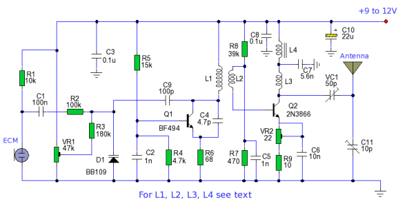
That’s why these circuits are more complex than just putting the components together and connecting a supply. 200mW FM TRANSMITTERThe power output of many transmitter circuits are very low because no power amplifier stages are incorporated. The transmitter circuit described here has an extra RF power amplifier stage, after the oscillator stage, to raise the power output to 200-250 milliwatts. With a good matching 50-ohm ground plane antenna or multi-element Yagi antenna, this transmitter can provide reasonably good signal strength up to a distance of about 2 kilometres.
Circuit Notes
The circuit is built around transistor T1 BF494. It is a low-power variable-frequency VHF oscillator. A varicap diode is included to change the frequency of the transmitter and to provide frequency modulation of the audio signals. The output of the oscillator is about 50 milliwatts. Transistor T2 2N3866 forms a VHF
“class A” power amplifier. It boosts the oscillator signal power four to five times. Thus, 200-250 milliwatts of power is provided at the collector of transistor T2.
For best results, construct the circuit on a PC board with all components closely connected and put the transmitter in an aluminum case.
Coil winding details::
L1 - 4 turns of 20 SWG wire close wound on 8mm diameter plastic former.
L2 - 2 turns of 24 SWG wire near top end of L1.
(Note: air core for the above coils)
L3 - 7 turns of 24 SWG wire close wound with 4mm diameter air core.
L4 - 7 turns of 24 SWG wire-wound on a ferrite bead (as choke)
- Potentiometer VR1 is used to vary the fundamental frequency whereas potentiometer VR2 is used as power control.
- For hum-free operation, connect the transmitter on a 12V rechargeable battery pack of 10 x 1.2-volt Ni-Cd cells.
- Transistor T2 must be mounted on a heat sink.
- Do not switch on the transmitter without a matching antenna.
- Adjust both trimmers (VC1 and VC2) for maximum transmission power.
- Adjust potentiometer VR1 to set the frequency to about 100MHz.
POWERING A BUG
It is always the best to power a bug from a battery. It keeps the whole project simple.
However if you want to power a bug for a long period of time, here is a circuit that will reduce the hum from a normal plug pack by a factor of about 2,000.
This means a 20mV ripple will be 1uV and will not be noticed. Any background hum is annoying and very difficult to remove with electrolytics. This circuit is the answer. The 1k and 100u form a filter that makes the 100u ten times more effective than if placed directly on the supply-line. The transistor reduces the ripple by a factor equal to the gain of the transistor - about 200. The result is a reduction by a factor of 2,000. The circuit is suitable for up to 100mA. A power transistor can be used, but the 1k will have to be reduced to 220R for 500mA output. The output of the circuit is about 0.6v less than the output of the plug pack.

An ELECTRONIC FILTER
Quick Links
Legal Stuff
Social Media


