Table Of Contents

Contents of Article
- Page 1: Basic Electronics
- The capacitor - how it works
- The Diode - how the diode works
- Every Circuit Symbols
- Soldering Videos
- Page 2: The Transistor
- PNP or NPN
- Transistor TEST
- Page 2a: The 555 IC
- Page 3: The Power Supply
- Page 4: Digital Electronics
- Page 5: Oscillators
- Page 6: Basic Electronics 50 Questions Test
- Page 7: using The Multimeter
- Page 8: Constructing a Project
- Page 9: Inductance
INDEX
Active
[Power](#Supply Rail)
THE TRANSISTOR
In this section we will cover THE TRANSISTOR.
The transistor is a 3-leaded device that comes in many different shapes and sizes with hundreds of different voltage and current and amplification values and capabilities.
There are 20,000 different types and we are going to concentrate on just TWO.
They are called NPN and PNP GENERAL PURPOSE TRANSISTORS.
Their technical name is BIPOLAR JUNCTION TRANSISTOR to distinguish them from other types of transistor such as Field Effect Transistor, Uni-Junction Transistor, and other types.
The transistor we will cover is used in hobby circuits. It is the cheapest, simplest and most-common transistor and has one of the following identifications (according to the country of origin).
NPN types include: BC547, 2N2222. 2N3904, PN100, BC338, 2SC945, BC107, BC147, 9013
PNP types include: BC557, 2N3906, PN200, BC157, BC327, 9012, 9015
99% of circuits use NPN transistors and this is the type we will describe. The PNP type is called a “mirror image” and we will explain it also.
This narrows the field to one type of transistor and we will describe over 100 different ways to use it in a circuit.
Before we start, we will show you the “end product.”
The following animation shows how a transistor works.
A drip entering the base (the funnel) will produce a “thump” from the speaker. A larger drop will produce a louder “thump.”
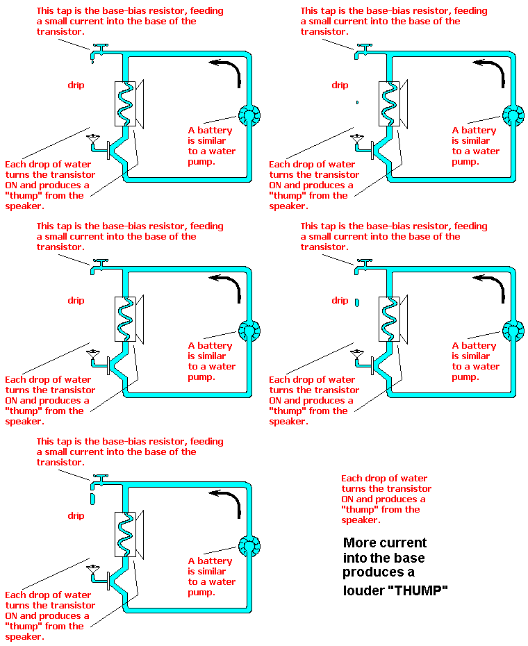
Fig 1. The WATER NPN TRANSISTOR
The animation shows a WATER NPN TRANSISTOR. The drip represent a small amount of energy entering the base (in the form of a voltage and current).
This results in a larger current flowing in the speaker.
As the drip gets bigger, the “Thump” from the speaker gets louder.
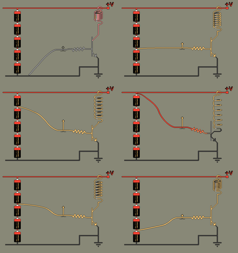
Fig 2. The SPRING TRANSISTOR
Here is a transistor animation from Williamson Labs: http://www.williamson-labs.com/480_xtor.htm
It shows a transistor being turned on by more current flowing into the base and this makes the transistor “squeeze tighter and pulls the spring “down.”
We will now explain how a transistor works.
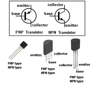
Fig 3. TRANSISTOR SYMBOL
The symbol for a PNP and NPN transistor are shown in the diagram.
As you can see, PNP and NPN transistors look exactly the same.
You need to identify them by the numbers on the side of the device or by testing them.
We have included a Transistor Tester in Fig 65 of the first section of the course.
The leads on a transistor can be:
emitter-base-collector
or
collector-base-emitter
and that’s why you have to know what to do.
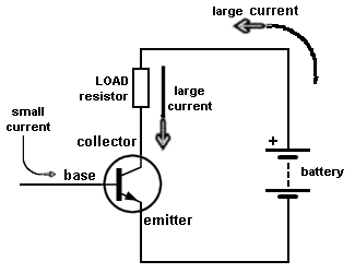
Fig 4. TRANSISTOR IN A CIRCUIT
The first type of transistor we are going to study is the NPN.
A transistor has three leads:
BASE, COLLECTOR and EMITTER
Basically, a small current enters the base and a large current flows through the collector-emitter leads as shown in the diagram.
The resistor in the collector lead is called the LOAD Resistor. Sometimes the load is a speaker.
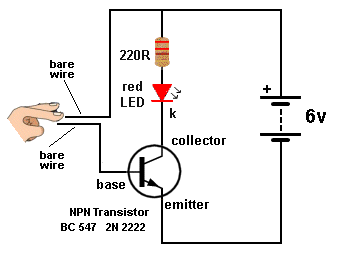
Fig 5. Turning ON a TRANSISTOR
Turning ON a TRANSISTOR
Here is a simple project to turn a transistor ON.
Touch the two bare wires with a finger and squeeze HARD.
Make sure the two wires do not touch as this will instantly damage the transistor.
The LED will illuminate very faintly as you press on the wires.
Your fingers allow current to flow through the two wires and into he base of the transistor.
The transistor amplifies this current and illuminates the LED. It will be very dull.
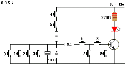
Fig5a. Which switches do you push (at the same time) to turn the transistor ON? (answer above)
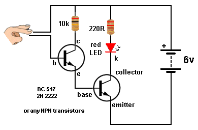
Fig 6. Two TRANSISTOR Circuit
By adding another transistor we amplify the current through the finger about 200 times and now the LED will glow bright.
The ACTION of the first transistor is to amplify the current through your finger.
This is sometimes called:
TRANSISTOR ACTION
It means the amplifying action of a transistor.
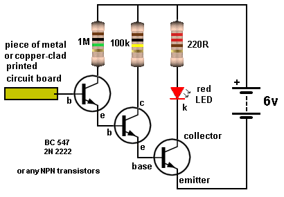
Fig 7. Three TRANSISTOR Circuit
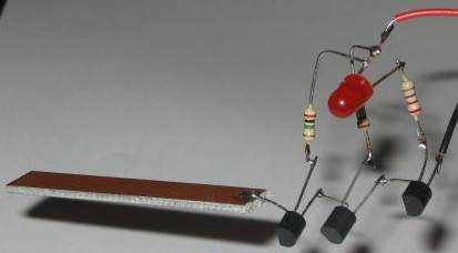
This circuit has enormous gain.
Each transistor has a gain or more than 200 and the final gain will be more than:
200 x 200 x 200 =
8,000,000
8 MILLION!
The circuit is very sensitive to static voltages in the air or electrical waves such as the waveform produced by the electrical wiring in a house.
Move the project around a room and detect all the electrical signals.
The circuit above is very simple but it shows how to connect 1, 2 and 3 transistors to produce a circuit with enormous GAIN.
GAIN is the AMPLIFICATION provided by each transistor. Some call it:
TRANSISTOR ACTION.
Turning ON a transistor is the most difficult part to understand so we will cover it in a completely new way. The animation below shows the transistor turning ON when the base voltage reaches 0.65v.
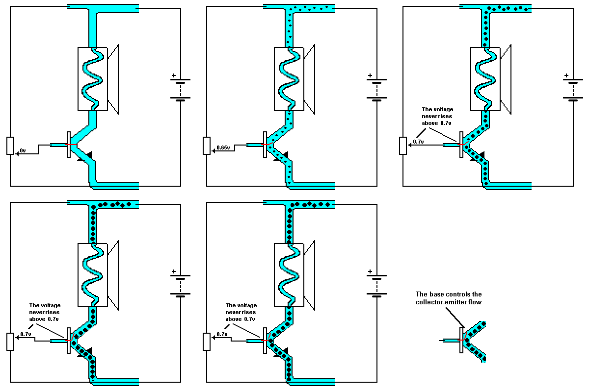
Fig 8. The Base turning ON a Transistor
The transistor does not turn on until the base voltage is 0.65v.
A small current into the base will produce a larger current-flow in the collector-emitter circuit.
As the potentiometer is raised, more current flows into the base and this causes more current to flow in the collector-emitter circuit.
The base voltage increases to a maximum of about 0.7v
The two facts we have covered above are:
- The transistor does not turn ON until the base voltage is 0.65v.
- The collector-emitter current increases if the base current increases.
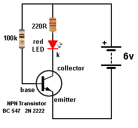
Fig 9. Base Bias
BASE BIAS
Instead of your finger turning ON the transistor (as shown in Fig 5 above), it can be turned on via a resistor.
This is called a BASE BIAS resistor.
Firstly it will provide the 0.65v to 0.7v for the base and secondly it will provide a current into the base.
The transistor will amplify this current about 200 times and the LED will illuminate.
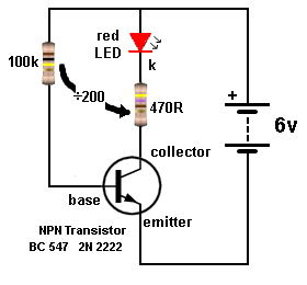
Fig 10. New Concept
Here is a new concept
To work out how the circuit will respond to a 100k base-bias resistor, we divide the 100k by the gain of the transistor. We assume the gain of the transistor in this circuit is 200.
100k / 200 = 500 ohms Use 470R resistor.
This is a quick. easy. simply way to “see” a circuit working.
The gain of a transistor can be 150 to 300 in this circuit so no amount of mathematics is going to produce a better result.
Note: this concept works when the new value of load resistor is larger than the old load resistor.
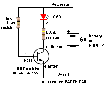
Fig 11. Circuit Names
The name of each component is identified in this figure.
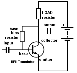
Fig 12. The self-biased Transistor
The self-biased Transistor
The self-biased transistor is an amplifier stage consisting of a transistor, base bias resistor, load resistor input capacitor and output capacitor.
It is called a STAGE because it has its own input and output capacitor and its own biasing.
The capacitors prevent any DC biasing on one stage from affecting the biasing of another stage.
In other words, this stage is self-contained.
How the self-biased Transistor Works
When the circuit is turned ON, the transistor is not conducting and the base sees a voltage and current via the base-bias resistor and LOAD resistor.
This turns the transistor ON. Current flows through the collector-emitter terminals and the same amount of current flows through the LOAD resistor. This creates a VOLTAGE-DROP in the LOAD resistor and the voltage on the collector drops. This means the voltage across the base bias resistor is reduced and this reduces the current into the base of the transistor.
This causes the transistor to turn OFF slightly.
The transistor settles to a condition where the current through the base-bias resistor allows say 200 times more current to flow in the LOAD resistor. A voltage develops across the load resistor to produce a condition called the QUIESCENT condition or IDLE condition or DC CONDITION.
The value of the two resistors are chosen so the voltage on the collector is mid-rail.
This allows the transistor to amplify both the positive portions (excursions) of the input waveform as well as the negative portions.
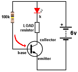
Fig 13. HOW MUCH CURRENT IS FLOWING?
HOW MUCH CURRENT IS FLOWING?
The current-flow into the base can be worked out by Ohm’s LAW
OHM’S LAW
Ohms Law is a simple equation that connects VOLTS, AMPS and RESISTANCE.
VOLTAGE is measured in VOLTS
CURRENT is measured in AMPS and
RESISTANCE is measured in OHMS OHM’S LAW TRIANGLE 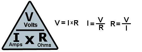
Cover the letter you want and the other two values appear in the correct place in the equation.
In the circuit above we know the value of voltage and resistance, so the equation is:
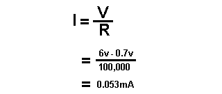
If the transistor can amplify this current 200 times, the collector-emitter current can be about
0.053 x 200 = 10.6mA

Fig 14. LOAD Current
The transistor is capable of delivering 10.6mA through the collector-emitter circuit but let’s look at what the 470R will deliver.
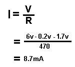
You can see the complexity of the mathematics. That’s why we will simplify the maths.
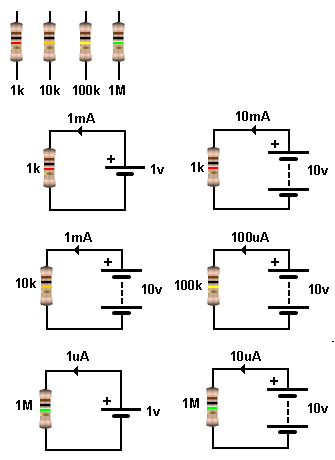
Fig 15. Simple Mathematics
Here is an easy was to work out the current flowing through a resistor.
- In the first circuit, a resistance of 1k will allow a current of 1mA to flow when the voltage is 1v.
- If the voltage is 10v, the current will be 10mA.
- For a 10k resistor, when the voltage is 10v, 1mA will flow.
- For a 100k resistor,
- 100 microamp will flow when the voltage is 10v.
- For a 1M resistor, the current will be 1uA for 1v supply and 10uA for 10v supply.
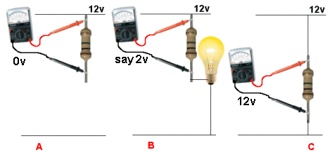
Fig 16. Voltage Drop
In our discussions we have talked about a LOAD resistor and when current flows through a resistor a voltage is developed across it.
In circuit A, the resistor is not connected and no current flows and it is not a load resistor (at the moment).
The globe in circuit B has a load resistor. The voltage across the resistor may be 2v, (depending on the value of the resistor). If a high voltage is developed across the resistor, the globe will not be very bright.In circuit C the resistor is connected across the rails and 12v will be across the resistor.
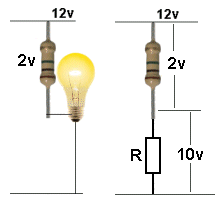
Fig 17. The Voltage Divider
In circuit B above, the resistor will have 2v across it and the globe will have 10v across it. The globe can be considered to be a resistor and thus we have two resistors in SERIES as shown in the diagram on the left.
The 12v is divided between the two resistors. It does not have to be divided equally.
But the voltage across the top resistor plus the voltage across the bottom resistor must equal the voltage of the supply.
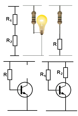
Fig 18. Types of Voltage Divider
A voltage divider can be two or more resistors in SERIES or a resistor and globe, or two globes or a resistor and a transistor.
The base-bias resistor R forms a voltage divider with the base-emitter junction.
The LOAD resistor R2 forms voltage divider with the collector-emitter terminals of the transistor.
Any two or more items in SERIES will produce a VOLTAGE DIVIDER.
The CURRENT (in Amps) through the top component will be the same as the current through the bottom component.

Fig 19. The STAGE
The circuit shown is called a ”STAGE.”
A Stage is a set of components (generally including a transistor) that is separated by a previous stage by a capacitor and has a capacitor on the output.
A capacitor does not allow DC (Direct Current) to pass through it and this really means the voltage on a previous stage is not passed to the stage we are analysing.
This means the voltage on or across each of the components is due to the biasing of the components in the stage we are analysing.
Ideally the collector should be at half-rail voltage and this is called the “idle” or “standing” or “quiescent” conditions.
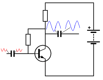
Fig 20. Signal Through A Capacitor
The voltage on one side of a capacitor may be 3v and 6v on the other side. The 3v can drop to 0v slowly and the 6v will not change. A capacitor does not pass DC.
But if a 3v signal is delivered to one side of a capacitor, the signal will pass through and appear on the other side.
The signal will be reduced a small amount but the main point to note it will PASS THROUGH THE CAPACITOR.
This is how an audio signal passes through an amplifier, from one stage the next and is amplified by each stage.
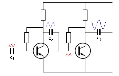
Fig 21. AC Coupling Two Stages
Combining the information we have learnt, we can combine two stages and show how the signal is amplified through two AC coupled stages.
Each stage consists of a self-biased transistor with a capacitor at the input and output.
This type of coupling is called AC COUPLING because it will only pass AC signals.
It is also called RC Coupling (Resistor-Capacitor coupling) and it only passes AC signals - fluctuating signals - rising and falling signals.
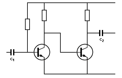
Fig 22. DC Coupling two Stages
Two stages can be DIRECTLY CONNECTED as shown in the circuit above.
This is called DIRECT COUPLING or DC COUPLING
DC actually stands for Direct Current. This sounds unusual, but it is the way to explain the circuit will pass (amplify) DC voltages and that’s why we say they are DC COUPLED. This type of coupling will pass both AC signals and DC voltages.
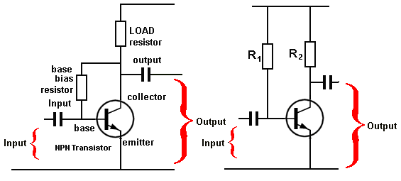
Fig 23. The Common Emitter Stage
The STAGES above are a COMMON EMITTER STAGE because the emitter is connected to the 0v rail and the input uses the base and the emitter and the output uses the collector and emitter, making the emitter COMMON to both the input and output.

Fig 24. The Common Collector Stage
The common Collector Stage is also called Emitter Follower Stage.
The COMMON COLLECTOR STAGE has the collector connected to the top supply rail and the input an output is shown on the diagram.
The top SUPPLY RAIL and the 0v rail connect to a battery or some other source of voltage and the resistance between the two rails is very small.
That’s why the input between the base and 0v rail can also be considered to be between the positive rail and base. The output can be considered to be between the emitter and positive rail. The collector is connected to the positive rail and it is effectively COMMON to the input and output.
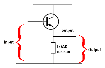
Fig 25. The Common Collector Stage is STRONG! The output is 100 - 200 times stronger than the input.
The COMMON COLLECTOR STAGE takes a weak input signal and delivers a strong output.
See animation.
The output can be abut 100 to 200 times stronger.
The output voltage is the same as the input voltage but the CURRENT is increased.
The emitter follows the voltage on the base ants why it is called an EMITTER FOLLOWER stage.
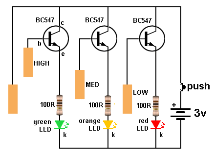
Fig 25a. Water Level Detector
Here is a circuit using an EMITTER-FOLLOWER stage to illuminate a LED when two probes detect water. There are three levels, High, Medium and Low.
Water has a resistance and when water touches the High pad and the pad on the left it is just like the Base-Bias Resistor shown in the circuits above.
The base-bias resistor turns ON the transistor and the base rises. The emitter “follows” and it rises too. This puts a voltage on the emitter which is passed through the 100R to the LED.
There are three separate identical circuits to show when the water tank is full, half-full and near empty.
Pure water has a very high resistance but the minerals in tap water make the water conductive.
Build the circuit and see the LEDs illuminate. You can see them gradually come ON as the water rises.
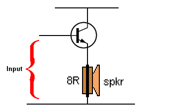
Fig 26. Driving a Speaker
A weak input signal can be converted to a strong signal by using an EMITTER FOLLOWER transistor to drive a speaker.
The transistor amplifies the strength of the signal by a factor of about 100 times.
The amplitude of the signal is not increased, just its ability to drive a current through a LOAD (the speaker).
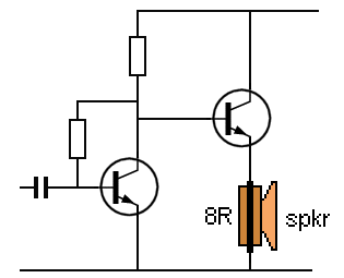
Fig 27. Connecting two Stages
The circuit shows how to connect two stages to drive a speaker.
A speaker is a very low impedance (resistance) device and a weak signal will not create any output.
The first stage is a self-biased common-emitter stage that will increase the amplitude of the signal about 100 times and also increase its strength.
The second stage takes the amplitude of the signal and delivers the same amplitude but with an increased strength of about 100 times.
What is a SIGNAL?
A Signal is an input voltage.
It may be the signal from an electret microphone, an audio waveform, or the resistance of your finger or a sinewave from a generator.
In all these instances we have described the amplitude of a signal. The amplitude is the VOLTAGE of the signal.
But a signal consists of a VOLTAGE and comes with a value of CURRENT. This current may be very small (such as from an electret microphone) or it may be very high (such as from a switch).
In most cases we do not talk about the value of current associated with the signal.
At this point we will simply say that ALL signals come with a VALUE OF CURRENT. And this is called “The Power of a SIGNAL.” In other words: The STRENGTH of a Signal” or the “Driving capability of a signal.
We can say a signal is “very weak” or “delicate” or “strong” or “has good driving capability.”
Some signals will drive a LED or speaker while others need to be amplified before they can be used.
In most cases the “driving power of a signal” is unknown. It is not provided as a specification. And yet its value is MOST IMPORTANT. In most cases you cannot work out the current-capability of a signal by looking at the device generating the signal.
That’s why we are showing how to amplify a signal so that it is strong enough to drive an output device.
This is a very complex area of discussion and we will introduce it slowly.
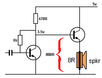
Fig 28. Voltages on the Circuit
(This circuit is only to show how to connect stages together. It is NOT a good design as you will see later in the course.)
There are 3 more points we can cover with this circuit.
Amplifying circuits are designed backwards. They are designed from the output to the input.
In this circuit the output is 8 ohms.
The emitter-follower has a gain of about 100 and this means the impedance of the speaker is reflected to the base by a value of 8 x 100 = 800 ohms.
The load resistor for the self-biased transistor must be 470 ohms so the voltage on the collector will be higher than mid-rail voltage.
The value of R1 can be 1M to 2M2 as the transistor is held at mid-rail by the second transistor and R1 will only be used to supply turn-on voltage for the base of the first transistor.
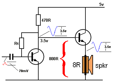
Fig 29. Signal Amplification
If the first transistor has a GAIN of 50, a 70mV input signal will produce
70 x 50 = 3500mV (3.5v) signal on the collector.
The second transistor will pass this 3.5v signal to the speaker with a “current capability” of 100 times greater than the signal on the collector of the first transistor.
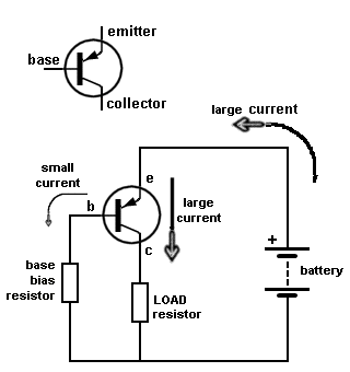
Fig 30. The PNP Transistor
The next set of circuits use both NPN and PNP transistors, so we need to explain how a PNP transistor works.
Basically it is a “mirror image” of an NPN transistor and is added to a circuit “up-side-down.”
The arrow on PNP transistor points to wards the base and follows the direction of current.
The Base Bias Resistor allows a small current to flow via the base and this creates a large current-flow though the emitter-collector terminals (emitter-collector junction).
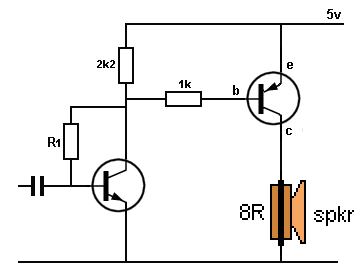
Fig 31. Connecting NPN to PNP
The speaker circuit in Fig 29 can be built with an NPN and PNP transistor, as shown opposite.
The 1k resistor is called a “stage separating resistor” or “stage joining resistor” or “current limiting resistor.”
It performs all 3 tasks.
It joins the to stages and limits the current through the emitter-base junction of the PNP transistor and collector-emitter junction of the NPN transistor when both transistors are turned ON.
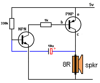
Fig 32. Creating an OSCILLATOR
If we connect a capacitor to the circuit in Fig 31, an amazing thing happens.
The circuit turns into an OSCILLATOR.
The circuit is actually a high-gain amplifier with POSITIVE FEEDBACK.
It introduces 3 new features.
Feedback can be POSITIVE or NEGATIVE.
Positive feedback takes a signal from the output of a circuit to an input and the result increases the amplitude of the signal on the input.
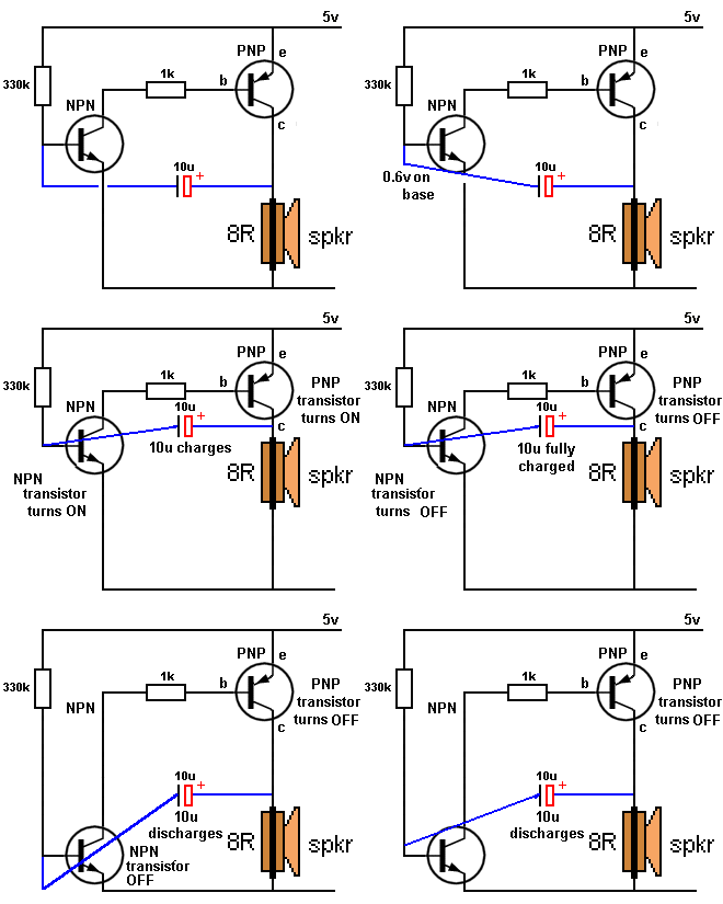
Fig 33. How the OSCILLATOR works
The 10u discharges through the base-emitter of the NPN and gets charged again via the 330k to start the next cycle.
The animation shows how the 10u charges via the 330k and when the voltage on the base of the NPN transistor is 0.65v, it turns ON and this turns on the PNP transistor via the 1k resistor.
The collector of the PNP transistor has about 3-4v on it and this makes current flow through the speaker to produce a “click.”
The positive lead of the 10u is taken HIGH and it starts to charge via the base-emitter junction of the NPN transistor.
When it is nearly charged, the NPN transistor turns off slightly and this turns off the PNP transistor and the voltage on the collector falls slightly.
This is passed to the base of the NPN transistor to turn it off slightly and the two transistors very quickly fully turn OFF.
The animation does not show the full complexities of how the oscillator works and one of the points to understand is the charging of the 10u.
At the beginning it gets charged in the reverse direction by the 330k and when the base of the NPN sees 0.65v, it starts to turn ON.
This causes the PNP to turn ON and the collector pulls the top of the speaker towards the positive rail. This action pushes the charge on the 10u into the base of the NPN transistor because the positive lead of the 10u rises and raises the negative lead. This immediately turns the NPN on MORE and very quickly both transistors are fully turned ON.
As the positive lead of the 10u rises a point is reached where the 10u changes from pushing its charge into the base to a point where it starts to charge in the forward direction because the positive lead is now higher than the negative lead.
During this time the current continues to flow into the base and that’s why the NPN continues to stay fully turned ON.
As the 10u charges, the current starts to decrease and a point is reaches where the flow of current into the base does not k\keep the NPN fully turned ON.
The NPN starts to turn OFF slightly and this is passed to the positive lead o f the 10u. The 10u “drops” slightly and this very quickly turns OFF the NPN and and the PNP.
They both turn off fully and now the base is a few volts lower than the 0v rail.
The 330k starts to remove the charge on the10u and eventually charge it to 0.65v to turn on the NPN to start the next cycle.
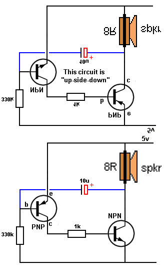
Fig 33a. INVERTING A CIRCUIT
An NPN transistor is a mirror image of a PNP transistor.
The circuit above can be “turned over” as shown opposite and the PNP transistor changed for NPN and the NPN transistor changed for PNP.
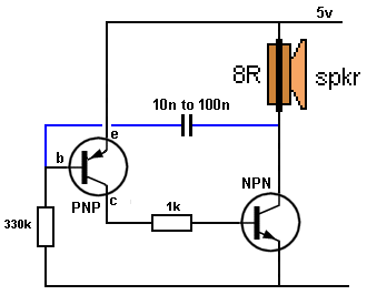
Fig 33b. Changing the Frequency
The frequency of the circuit can be increased by replacing the 10u electrolytic with a 10n to 100n capacitor.
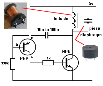
Fig 33c. Adding an INDUCTOR
If we replace the speaker with an inductor an amazing thing happens.
The inductor is just like a speaker but it has more turns and the effect we will be observing will be INCREASED.
To hear what the inductor does, we put a piezo diaphragm across it.
The piezo diaphragm detects voltage.
When the circuit it is turned ON the squeal from the piezo is VERY LOUD, indicating the inductor has increased the voltage.
An inductor is a coil of wire wrapped around a core made of iron or similar material.
It is also called a CHOKE or COIL.
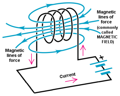
Fig 33d. Magnetic Lines of Force produced by an Inductor when a current flows
When current flows through an Inductor Magnetic Lines of Force are created.
The Inductor is turned into an ELECTROMAGNET and it will pick up small nails and pins.
But in the circuits we are describing, the amazing thing is when the inductor is turned OFF.
It produces a very HIGH VOLTAGE when it is turned OFF.
This voltage is due to the rapid collapsing of the magnetic field.
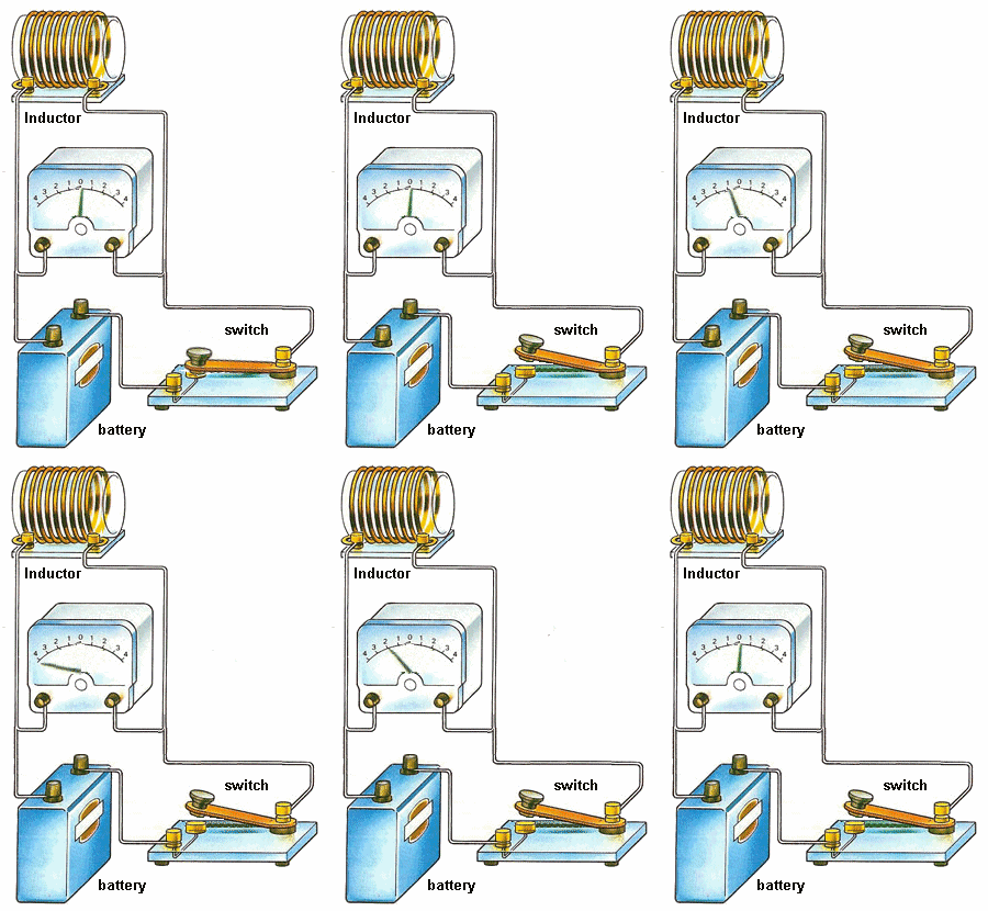
Fig 33e. Back Voltage - commonly called FLYBACK VOLTAGE
The animation shows the coil receiving a small positive voltage via the switch and when the switch is released, the coil (inductor) produces a very large voltage in the opposite direction.
The most important part of this animation shows the REVERSE VOLTAGE produced by the Inductor.
This is referred to as BACK EMF or FLYBACK VOLTAGE and is one of the most important facts to remember as it will allow you to understand how many circuits work.
It explains how a reverse voltage is produced in many circuits to illuminate LEDs etc.
We have shown how components such as capacitors and coils can COMPLETELY change the operation of a circuit. These components appear to be very simple but the way they work is very complex.
For example a capacitor can detect the change in voltage on one part of a circuit and send this change to another part of the circuit. This is commonly called FEEDBACK and can be POSITIVE FEEDBACK or NEGATIVE FEEDBACK.
A capacitor can do more than 10 other things, depending on where it is placed and it size.
A coil (inductor) is more complex than you think. It can also perform more than 10 different effects, depending on its size and where it is placed.
If another coil of wire is placed on top of the first coil, it becomes a TRANSFORMER and this will be discussed later.
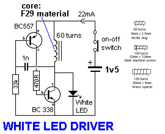
Fig 33f. Flyback Circuit
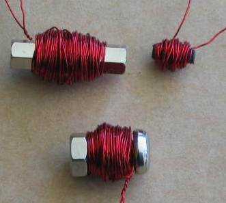
Here is a circuit that will illuminate a white LED from a 1.5v supply. We know a white LED needs 3.6v to illuminate so the added voltage must come for the “back voltage” produce by the coil. The 60 turn inductor is wound on a small ferrite slug 2.6mm dia and 6mm long with 0.25mm wire.
The main difference between this circuit and the two circuits above is the use of a single winding and the feedback to produce oscillation comes from a 1n capacitor driving a high gain amplifier made up of two transistors.
The feedback is actually positive feedback via the 1n and this turns on the two transistors more and more until finally they are fully turned on and no more feedback signal is passed though the 1n. At this point they start to turn off and the signal through the 1n turns them off more and more until they are fully turned off.
The 33k turns on the BC557 to start the cycle again.
If you do not have a ferrite slug, the inductor can be made from a machine screw 10mm long and about 3-4mm dia. Wind 150 turns of 0.25mm wire. Or you can use a brass ferrule 20mm long x 5mm. Wind 150 turns.
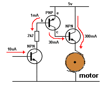
Fig 34. Driving a Motor
We can combine the last three stages we have covered and combine them to produce a circuit to drive a motor.
A circuit to drive a motor needs a high current on the output.
This circuit takes a very weak input signal of 10uA and amplified it via the first transistor, about 100 times to provide 1mA base current for the second transistor. The second transistor amplifies the current abut 30 times to provide 30mA for the emitter-follower and the output of this transistor will deliver about 300mA to the motor.
The 3 stages above are DC COUPLED to each other and any signal above 0.65v on the input of the first transistor will turn it ON. 10uA is a very small current so that almost any signal will activate the circuit.
The 2k2 resistor limits the current through the emitter-base junction of the PNP transistor and 1mA is enough to turn it ON fully.
The PNP transistor will deliver at least 30mA to the base of the third transistor and this will provide more than 300mA for the motor. The current taken by the motor will depend on the loading of the motor and the circuit must be able to deliver this current.
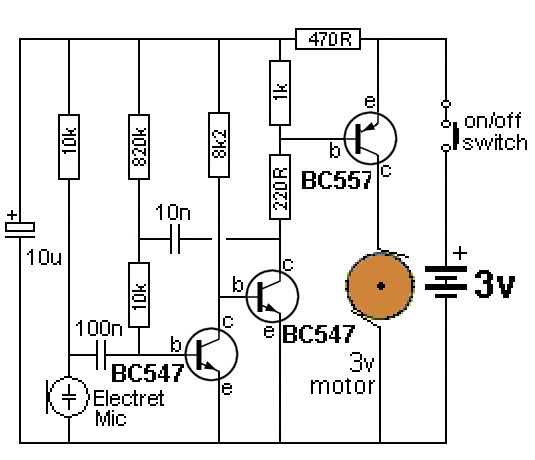
Fig 35. Dancing Flower

Dancing Flower
Here is a practical circuit using the “building Blocks” we have covered.
The second and third transistors form the high-gain amplifier described in Fig 31 and the first transistor is a COMMON EMITTER STAGE described in Fig 23.
But we have an added component. A 10n capacitor. We have already explained that a capacitor can provide FEEDBACK - POSITIVE FEEDBACK and that is what this capacitor does.
The capacitor does not make the circuit oscillate but it provides a feedback pulse that turns the circuit ON FULLY when a small pulse is received from the electret microphone.
A small negative waveform through the 100n will turn the first transistor off slightly and the collector voltage will increase. This will turn on the second transistor slightly more and the collector voltage will drop. This will be passed to the right lead of the 10n capacitor and the left lead will also drop. This will put a lower voltage on the base of the first transistor and it will turn off more.
At the same time, the lower voltage on the collector of the second transistor will be passed to the base of the third transistor to turn it ON and the increased voltage on the collector will spin the motor.
The 10n will gradually charge and the first transistor will turn ON and this will turn OFF the second transistor and the motor will stop.
Music picked up by the electret microphone will make the motor start and stop to make the flower wiggle.
The motor is slowed down via a gearbox and a shaft is passed up the stem of the flower. The shaft is bent so that when it rotates, the flower dances like a hoola hoola dancer.
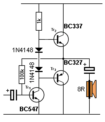
Fig 36. Push-Pull
You will recognise some of the sections of this circuit, but the transistors work in a slightly different way to the previous circuits we have described.
The new items are the diodes.
Both the diodes are “turned ON” and conducting. The voltage across each diode is 0.65v.
The voltage across a base-emitter junction of a transistor needs to be about 0.7v for the transistor to be conducting. This means the diodes are at the point of just preventing the transistors turning ON.
When the BC547 receives a negative signal, it turns OFF and the 1k resistor pulls the BC337 towards the top rail and the emitter-follows and pulls the positive of the electrolytic HIGH. This starts to charge the electrolytic and the charging current flows through the speaker.
When the BC547 receives and positive signal, it turns ON and pulls the base of the BC327 towards the 0v rail and the emitter follows and pulls the positive lead of the electrolytic towards the 0v rail. This discharges the electrolytic and the discharge current flows through the speaker in the opposite direction to move the cone in the opposite direction.
At the same time the two diodes pull the base of the BC337 towards the 0v rail and it gets turned OFF.
The circuit is called PUSH PULL because it pushes the energy in the electrolytic through the speaker and then pulls then pulls the energy from the electrolytic via the speaker.
The current and voltage of the incoming signal is increased by the first transistors and the other two transistors only increase the current-capability of the signal.
The PUSH PULL section is also called a COMPLEMENTARY-SYMMETRY output stage.
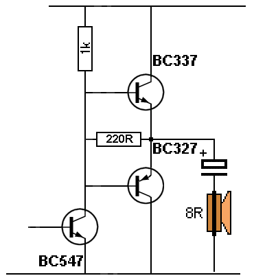
Fig 37. Current Dumping
Fig 37 shows a very clever variation of the Push-Pull circuit described above.
It uses a low-value resistor between the collector of the driver transistor and output. This resistor transfers the low-level signals directly to the speaker. As the signal-level increases, the output transistors come into operation.
This arrangement removes cross-over distortion and uses less parts.
It is called CURRENT DUMPING.
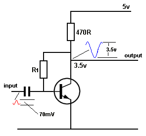
Fig 38. The Analogue Transistor
The transistor can be used in two different types of circuits.
- ANALOGUE CIRCUITS
- DIGITAL CIRCUITS
When the transistor is in an Analogue Circuit, we know it will be amplifying signals that are slowly rising and falling - such as audio signals.
We say it is an analogue transistor so we are ready to expect the voltages and waveforms on the base and collector when making tests.
DIGITAL ELECTRONICS
Digital Electronics revolves around circuits that are either ON or OFF. In other words they are in a HIGH state or LOW state.
Go to the DIGITAL section of the course for more on this topic.
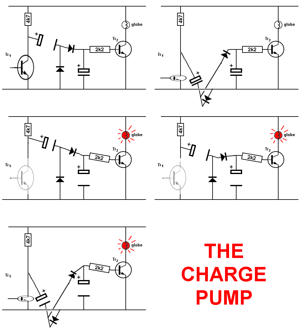
THE CHARGE PUMP
This circuit has a number of names and uses the amplitude of a signal to charge a capacitor.
The voltage on the capacitor is applied to the base of a transistor and the transistor turns on a LED, relay, globe or motor.
HOW A TRANSISTOR TURNS ON
When a transistor turns ON, it is just like a resistor having a smaller and smaller value of resistance. But the way it works in a circuit and the “effect” on other components can be different. Here are animations to show how a transistor can be turned ON:

SIMPLE AMPLIFICATION
The finger is just like a resistor. As you press harder, the resistance gets smaller and the transistor turns ON more.
This is because more current flows from the positive rail and into the base of the transistor. The transistor amplifies this current and allows more current to flow in the collector-emitter circuit. The LED is in the collector-emitter circuit and it gets more current. This makes it glow brighter.
CUT-OFF and SATURATION
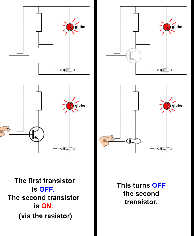
In this animation we see the first transistor turning OFF the second transistor. This action will be covered in more detail in the TRANSISTOR chapter.
At the moment, we just need to see is it possible to turn ON a transistor via a finger and this transistor will turn OFF the second transistor because it “robs” (takes away) the 0.6v (the base voltage) needed to start to turn ON a transistor.
The second transistor is receiving two different signals. The first signal consists of a voltage above 0.6v and current from the LOAD resistor to turn it ON (it is SATURATED). After the finger is applied, the second signal consists of a voltage less than 0.6v and the transistor is CUT-OFF (does not work). (There is no regeneration or feedback in this circuit.)
REGENERATION due to FEEDBACK
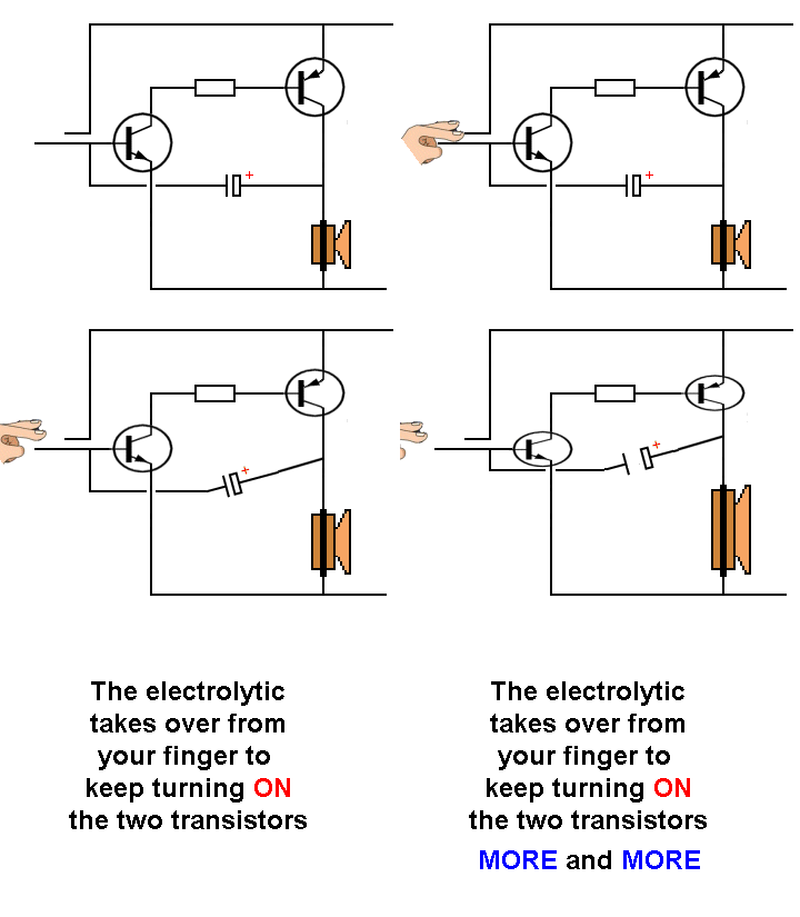
When two transistors are connected so one transistor turns ON the second transistor and the second transistor FEEDS-BACK to the first transistor to turn it ON MORE, the action is called REGENERATION.
It is just like “face-slapping.” It starts with a slight slap, and it gets stronger and

stronger until both transistors are FULLY TURNED ON.
Regeneration can apply to a single transistor where a percentage of the output is fed back to the input to increase the amplitude of the signal or it can apply to two transistors where the feedback is provided by a capacitor (electrolytic).
Regeneration is a feature called POSITIVE FEEDBACK and the circuit turns itself ON more and more. Generally it only requires a very small signal to start the action.
This animation shows how a finger starts to turn ON the first transistor. The first transistor turns ON the second transistor and the output of the second transistor is FED BACK to the first transistor to turn it ON more.
You can see the finger is removed very quickly and the action continues due to FEEDBACK.
The circuit is a HIGH GAIN DC AMPLIFIER with POSITIVE FEEDBACK.
At the moment we are only interested in seeing how the circuit keeps turning itself ON more and more …
TURNING ON an EMITTER-FOLLOWER
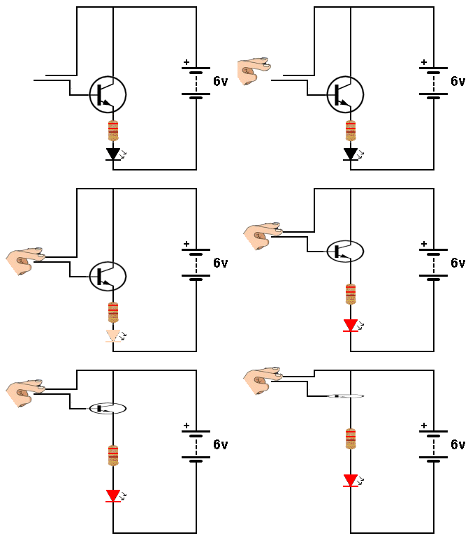
When a LED is in the emitter lead of a transistor, it will be illuminated when a finger touches the wires shown in the following animation:
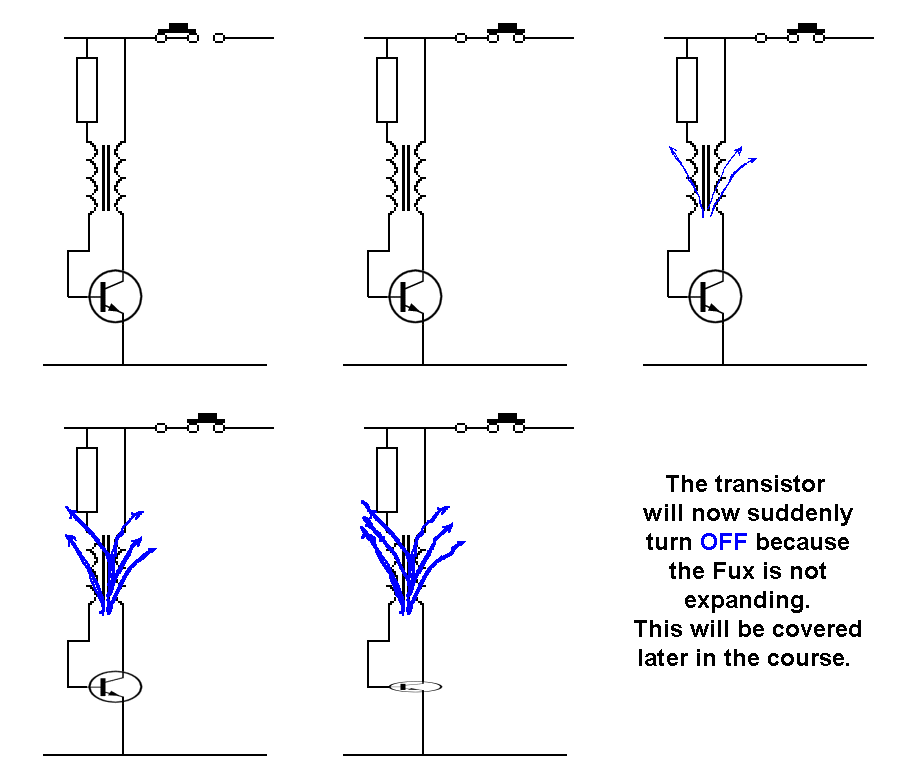
FEEDBACK via a TRANSFORMER
A transistor can be turned on via a positive FEEDBACK winding of a transformer. This is a winding that supplies voltage (and current) to turn the transistor ON harder.
The transformer turns the transistor ON fully then IMMEDIATELY stops turning it on.
This is one of the amazing features of a transformer when connected as shown in the diagram and you will learn more about this in the course.
At the moment, we are only describing the TURN ON of the transistor and the fact that as soon as it is fully turned ON, the transformer stops turning the transistor ON. This is because the expanding flux suddenly stops when the transistor is fully turned ON and the feedback winding ceases to supply energy to the base.
PNP TRANSISTOR
A PNP transistor is a mirror-image of an NPN transistor and is turned ON by a finger as shown in this animation:
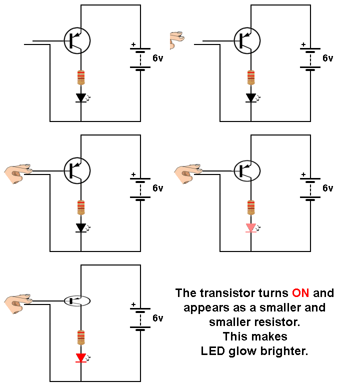
These animations are designed to help you “SEE” a circuit working. They represent a visual indication of how an electronics engineer sees a circuit in operation. He sees every part of a circuit working and moving and when a fault develops, he can SEE WHY!
These animations only show half a cycle.
The other half-cycle turns the transistor OFF (referring to the Regeneration and Feedback via a Transformer animations). Turning the circuit OFF is complex and will be covered in a future chapter.
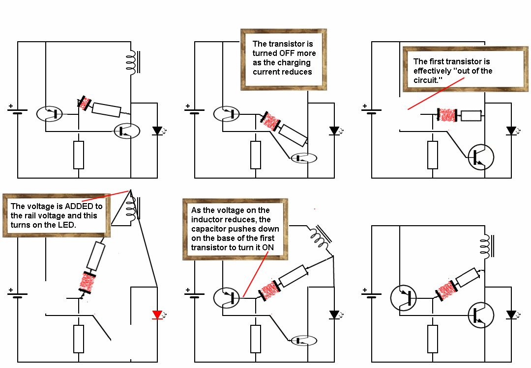
This animation shows many of the features we have covered.
It is very difficult showing an animation because some of the components are reacting to voltage-changes and some to current changes (the transistors).
That’s why you need to study many different animations from different circuits to be able to generate a picture of how a circuit is working.
In this animation we have an inductor, a capacitor and two types of transistors.
HOW THE CIRCUIT WORKS:
The circuit turns ON via the 220k resistor and the voltage on the collector of the NPN transistor drops to nearly 0v. This action causes current to flow through the inductor and at the same time the 1n capacitor is brought towards the 0v rail and this turns ON the first transistor slightly harder. This action continues until the driver transistor cannot be turned on any more.
The 1n charges a little more and the current through the base lead reduces slightly. This action turns OFF the first transistor slightly and the driver transistor is turned OFF a slight amount.
The voltage on the 1n rises and very soon both transistors are fully turned OFF.
The magnetic flux in the core of the 1mH inductor collapses and produces a voltage in the opposite direction.
This voltage is added to the 1.5v rail voltage and the final voltage is high enough to illuminate the white LED (approx 3.6v).
This keeps both transistors OFF and when all the magnetic flux has been converted to energy to illuminate the LED, the voltage on the collector drops. This lowers the top plate of the capacitor and since the capacitor is slightly charged, the bottom plate drops to a voltage less than rail voltage. This action turns ON the first transistor to start the next cycle.


Turning ON a transistor is more complex than shown in the animations. A transistor is turned ON when the base sees a voltage higher than 0.6v and the voltage will also allow a CURRENT to be delivered. These two requirements are normally provided in a circuit and your finger pushing on two wires will provide the voltage and current.
Here is an animation of what your finger is doing:
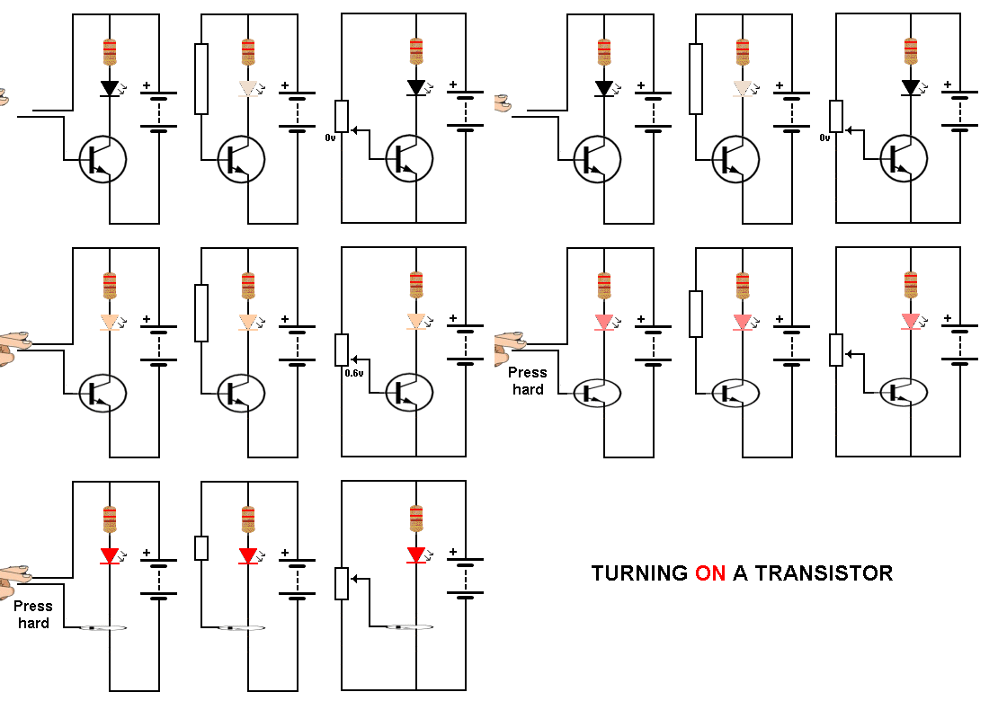
Pressing hard on the two wires is the same as reducing the value of the base resistor or turning the potentiometer. The action allows more current to enter the base of the transistor. The transistor amplifies this current about 100 times and illuminates the LED.
We have shown how to turn on a LED with a transistor.
A LED takes about 20mA and it’ s easy to illuminate with a transistor because 20mA is a small current and any transistor will deliver this current.
But suppose we want to illuminate a 6v torch globe that takes about 500mA when fully illuminated.
Some transistors only allow about 100mA to flow through the collector-emitter junction and they will either get too hot or “burn-out” when 500mA is flowing.
You need a transistor that allows more than 500mA to flow.
The two transistors will will use are BC337 (BC338) and 2N2222A. These transistors will pass up to 800mA without being damaged.
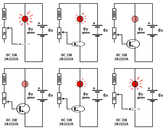
The BC 338 transistor handles the globe current
DIM A TORCH GLOBE
Connect the globe to the transistor and uses a 10k mini trim pot to adjust the base current. The 100R is called a “STOP RESISTOR” to prevent too much current flowing into the base and destroying the transistor. > Connect the circuit and turn the pot to zero ohms so that just the 100R is supplying current to the transistor. Feel the transistor.
Now turn the pot a small amount and keep feeling the transistor.
The lamp will be at about the same brightness but the transistor will get hotter. Move the pot a few more degrees and the transistor will get much hotter.
Keep turning the pot and the transistor will get much hotter when the globe is quite dull.
We will discuss the reason why it gets hot in a future lesson .
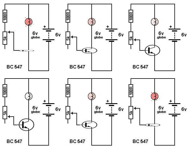
A BC 547 will not handle the globe current.
Connect a BC547 transistor to the circuit and turn the pot to zero ohms to get the lamp as bright as possible. Feel the heat of the transistor.
It will be much hotter than the BC337 and the lamp will not be very bright.
The transistor cannot pass the required current. You are overloading the transistor and is will possibly burn out.
This transistor is not suitable for the application.
Do NOT try to reduce the brightness of the globe by connecting just the pot to the globe. The pot will “burn-out” very quickly. You must always include the transistor.
All the globe current cannot go through the pot as this will burn the track inside the pot.
The transistor allows only 1/100th of the globe current to pass through the pot.
A BC337 transistor has a larger amount of silicon in the junction(s) and that is why it will pass (handle) a larger current.
- The transistor is coolest when it is illuminating the globe with full brightness.
- The transistor must be able to handle the globe current.
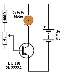

MOTOR SPEED CONTROL
The RPM (commonly called the “speed”) of a motor can be varied by the circuit shown.
You will need a 3v to 6v motor and 4 wheels on a chassis. The car in the photo is available as a kit from eBay.
Add the circuit and use a mini trim pot to adjust the speed.
<!-- TODO FIXME COLIN: Find missing article data -->
TRANSISTOR TESTER - 22
Here is a
Quick Links
Legal Stuff
Social Media


