Table Of Contents

We cover 5 of the most important oscillators and include the Fly-back oscillator (no text book has covered it!)
Contents of Article
- Page 1: Basic Electronics
- The capacitor - how it works
- The Diode - how the diode works
- Every Circuit Symbols
- Soldering Videos
- Page 2: The Transistor
- PNP or NPN
- Transistor TEST
- Page 2a: The 555 IC
- Page 3: The Power Supply
- Page 4: Digital Electronics
- Page 5: Oscillators
- Page 6: Basic Electronics 50 Questions Test
- Page 7: using The Multimeter
- Page 8: Constructing a Project
- Page 9: Inductance
INDEX
Active
Astable Multivibrator
Attenuate
Astable Multivibrator
Bootstrapping
Colpitts Oscillator
CRO - Cathode Ray Oscilloscope
Feedback
[Feedback Oscillator](#Feedback Osc)
Flip Flop
Free-Running Oscillator
Hartley Oscillator
Hysteresis Gap
Input Voltage Gap
Negative Feedback**
Hartley Oscillator
Hysteresis Gap
Input Voltage Gap
Negative Feedback**
Phase Shift
Positive Feedback
[Power](#Supply Rail)
Regenerative Feedback
Schmitt Trigger
**
OSCILLATORS
An Oscillator is a circuit that produces an OUTPUT - an output is a waveform (a signal, an amplitude). The output is produced by the components within the oscillator circuit. This circuit is generally shown as a rectangular BLOCK on a circuit and the actual components are shown else-where.
Sometimes a CONTROL-LINE enters the “block” to stop the oscillator, (called the HALT or FREEZE line) but generally the oscillator produces an output at all times.
We are going to look inside this “block” and see the components and how they produce the waveform.
Oscillators can be produced with transistors, Integrated Circuits (and surrounding components), OPerational AMPlifierS or dedicated chips. We will be studying circuits using transistors.
Oscillators use either or both ANALOGUE and DIGITAL circuitry to produce an output. Analogue circuitry is slow rising and falling waveforms and Digital circuitry is fast rising and falling waveforms.
A sine wave oscillator is considered Analogue (because the rise and fall of the waveform has a slope when seen on a Cathode Ray Oscilloscope). A Square-wave is considered Digital because the rise and fall is very rapid.
Some oscillators produce a sine-wave and some produce a square-wave. Others produce a “ramp” output (called a “saw-tooth”) and you can even get a noisy oscillator producing “white noise.”
The main criteria of an oscillator is the repetition-rate. It produces the same type of output (the same waveform) at a constant rate.
The rate is called cycles per second and this is given the name Hertz.
1 cycle per second = 1 Hz.
An oscillator must consist of, or contain, 3 sections (or features):
- An Amplifier,
- A Wave-Shaping Network, more-commonly called a TIMING NETWORK.
- Positive Feedback (to keep it oscillating)
Oscillators are used everywhere and can be used for counting, producing a tone, driving a motor, relay, transformer, speaker, piezo, LED, transistor and many other devices.
Generally an oscillator needs no input signal. It uses POSITIVE FEEDBACK within its own circuit to keep oscillating and the frequency at which it oscillates depends on the components in the circuit.
The transistor or Operational Amplifier or Integrated Circuit provides the amplification.
The wave-shaping components generally consist of resistors and capacitors or an inductor and capacitor(s). These components determine the frequency at which the circuit will oscillate.
They form a TIME DELAY and the rate at which the capacitor charges and discharges creates the delay and the shape of the waveform.
The positive feedback is generally a capacitor connected to a rising signal and takes this rising signal to a previous section of the circuit where it will INCREASE the waveform and assist in the operation of the circuit.
Some oscillators are very simple while others are very complex.
Some are easy to understand and that’s where will start.
The simplest oscillator is the FLIP FLOP.
It consists of two transistors and a few passive components (resistors and capacitors) and is very reliable. It always works.
In its simplest form it drives two LEDs with alternate blinking, like a railway crossing signal.
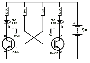
Fig 1. The FLIP FLOP
or Astable Multivibrator
or “free-running” Multivibrator.
The FLIP FLOP is a multivibrator circuit that will alternately flash the two LEDs.
It is called an ASTABLE MULTIVIBRATOR and this means it is not stable but keeps switching from one transistor to the other.
Multivibrator means “more than one amplifying device” and in this case it uses two transistors.
”Multivibrator” originally meant the output was rich in harmonics.
“Multi” means: many, and “vibrator” means: movement.
Astable is “Aye-stable”
not: As-table.
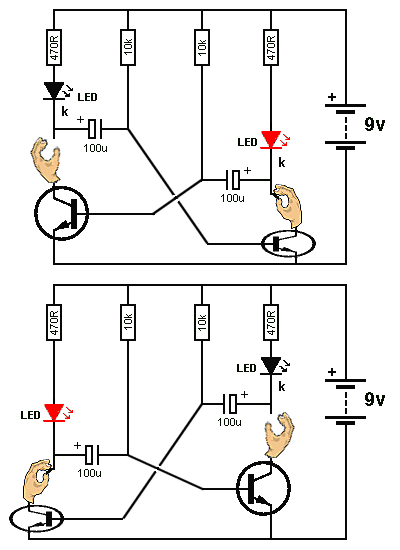
**Fig** 2. The FLIP FLOP Animation
The FLIP FLOP in action, showing the each transistor turning ON and pulling the cathode (k) of the LED towards the 0v rail to turn it ON.
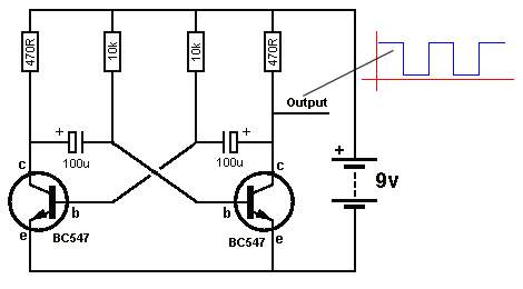
**Fig** 3. The Output Waveform of a Flip Flop
The output of the Multivibrator is a SQUARE WAVE. In this circuit the output is HIGH for the same length of time as the LOW because the 100u and 10k timing components are the same for each transistor. The diagram shows the output of the multivibrator can be taken to another “Building Block” such as an amplifier with speaker to produce a tone.
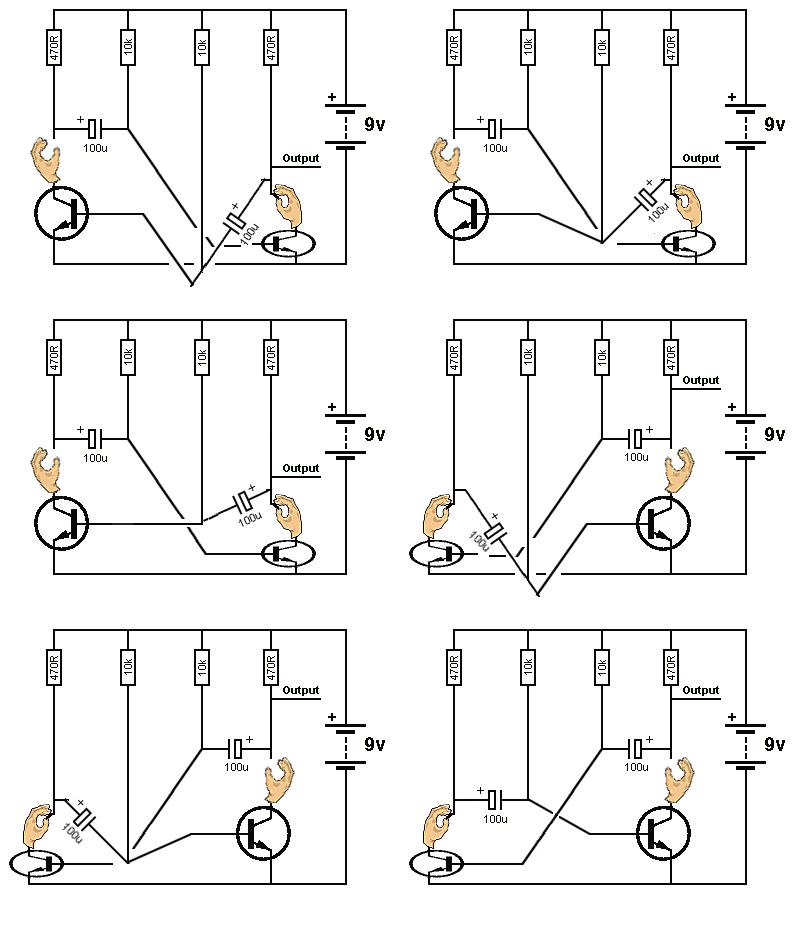
**Fig** 4. Flip Flop Animation-2
The animation of the Flip Flop shows the output rising and falling. The voltage on the capacitors (electrolytics) show the base going below 0v rail. The operation of the circuit is basically two TIME DELAYS and this has been covered in the Basic Electronics section of the course.
The Flip Flop produces a very clean output with a fast rise and fall time.
To increase the output frequency of the Multivibrator circuit, the capacitor values are reduced. When they are a small value, we can also reduce the value of the timing resistors to get even- higher frequencies.
The POSITIVE FEEDBACK of the Flip Flop circuit comes from the action of the capacitors. When the positive lead of the electrolytic moves in the “up” direction, it also moves the negative end “up” and provides a considerable effect on the base of the other transistor. The transistor amplifies this effect and the action is passed back to the first transistor and “around the circuit” very quickly. The end-result is the two transistors COMPLETELY change state. This action is called REGENERATIVE FEEDBACK because the feedback gets “more and more” as it passes from one transistor to the other.
The FEEDBACK action starts by one of the 10k resistors charging the 100u and removing the negative voltage it is supplying the base of the opposite transistor. The transistor is being kept OFF by the voltage on the negative lead of the 100u going BELOW 0v. The 10k gradually charges and removes this negative voltage and eventually the base voltage is 0.6v. This starts to turn ON the transistor and the 100u on its collector drops a small amount. This drop is sent directly to the base of the opposite transistor where a slight drop in voltage on the base will start to turn it OFF.
This makes the original 100u rise and the base of the transistor connected to the 100u will get more turn-ON current. This action goes around the two transistors very quickly until both have completely changed states.
POSITIVE FEEDBACK
means the feedback will produce a larger waveform.
NEGATIVE FEEDBACK
sends a signal from an output to an input that REDUCES the signal.
Negative Feedback is used in amplifiers to reduce distortion. It works like this: Distortion signals and noise-signals have a higher amplitude than the frequency being process and Negative Feedback has a greater effect on reducing the peaks of a signal. That’s why Negative feedback reduces the distortion.
By using smaller-value capacitors, the frequency of the circuit can be increased. This circuit is generally called a Multivibrator (Astable Multivibrator - Free-Running Multivibrator or ”Oscillator”).
The output is called a CLOCK or CLOCK LINE and is used in a computer to control the flow of data. The CLOCK LINE is taken to a number of chips in a computer to control the flow of information (data).
The multivibrator has many advantages. It only needs resistors and capacitors in the timing circuit and these can be fabricated into an integrated circuit. It is cheap, compact, easy to make, has a fast rise and fall time and produces a high output voltage and current.
Other oscillators need a coil and this is a large component.
There are four other simple oscillator circuits.
The Colpitts and Hartley oscillators are very simpler and both need an oscillator coil.
They work on another amazing feature of electronics.
When a coil and a capacitor are connected in series or parallel, and connected to a battery very briefly, the two components will pass energy from one to the other. In the case of the series components, the two ends have to be connected, but the parallel components will work perfectly.
A coil is classified as a passive component as it is not like a transistor and does not provide any amplification. A capacitor is also a passive component.
But when you place the two components together and briefly connect them to a battery, they pass energy back and forth in the form of a SINEWAVE.
This amazing feature is the basis of radio transmission and also many types of oscillator.
The Colpitts Oscillator uses a single coil and two capacitors, while the Hartley Oscillator uses a single capacitor and two coils. The two coils are wound on the same core in the form of a single coil with a centre-tap.
The third Oscillator we will cover is the Crystal Oscillator. It uses the natural oscillation of a crystal and the gain of a transistor to produce a frequency that is very stable. It is the most stable of all oscillators.
The transistor in a Colpitts Oscillator is just an amplifier. The oscillating components are the coil and capacitor combination.
The transistor simply delivers a small pulse of energy to the combination and they produce a sine-wave at the particular frequency. The waveform will gradually get smaller and smaller, so the output is sent to the transistor to turn it on for a period of time during a part of the cycle, so the output remains large.
The coil and capacitor have a special name: TANK CIRCUIT and this name came from early radio days when the circuit was used to transmit radio waves and the inventors considered the circuit held some of the energy and released it during part of the cycle just like a storage TANK.
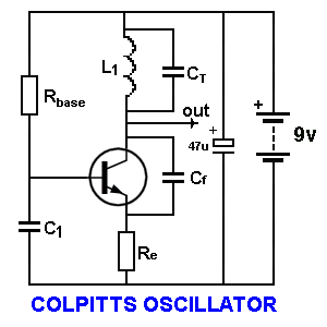
The circuit shows the simplest Colpitts Oscillator. The essential components are:
- The transistor - provides the amplification,
- The TANK CIRCUIT consisting of the coil L1 and Capacitor CT - starts the circuit oscillating.
- The base resistor, turns the transistor ON.
- Capacitor C1 prevents the base moving up and down and turns the transistor into a COMMON BASE configuration.
- The feedback capacitor Cf.
- The emitter resistor Re keeps the emitter away from the 0v rail so the feedback signal can be delivered to the emitter via the feedback capacitor Cf.
- The electrolytic (47u) across the power rails to keep the rails “tight.”
HOW THE CIRCUIT WORKS
The circuit starts by the transistor being turned on via the base resistor.
This puts a pulse of current through the coil and at the same time the capacitor CT charges. As the capacitor charges it allows a voltage to appear across the coil and this produces expanding magnetic flux. As soon as the capacitor stops charging, the magnetic flux stops and now it starts to collapse and produce a voltage across the coil in the opposite direction.
This voltage ADDS to the supply voltage and it passes through the feedback capacitor Cf to raise the voltage on the emitter. Because the base cannot rise or fall, the increased voltage on the emitter has the effect of reducing the voltage between the base and emitter and turns the transistor OFF slightly.
The voltage on the output pin rises slightly above rail voltage and charges CT until all the magnetic flux has been used. The voltage in CT is then delivered to the coil to produce more expanding flux to repeat the cycle.
As you can see, the circuit is much-more complex than first imagined.
Here are the main points to remember:
The coil and capacitor CT form a circuit known as TANK CIRCUIT and when a small pulse of energy is delivered to the parallel components (no other components in the circuit) they will produce an output that is a perfect sinewave. This is the amazing feature of two seemingly simple components. They produce a beautiful sinewave that gradually decays to zero.
This feature was the beginning of radio transmission as it allowed a radio station to transmit on a particular frequency and not all over the band. Previously, spark transmitters transmitted all over the band and no other radio station could transmit a the same time.
A Tank Circuit produced a TUNED CIRCUIT and this means the transmission was on a particular frequency so that much less energy was required to transmit much further.
Because one end of the tank circuit is held rigid by the supply rail, the other end rises and falls and this waveform is passed through the feedback capacitor to turn the transistor ON and OFF.
The Colpitts oscillator can also have two capacitors across the coil and the mid-point is passed to the transistor as the FEEDBACK LINE to turn it ON and OFF.
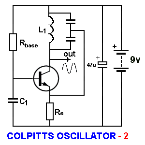
Both circuits are identical in operation. The value of the capacitors in parallel will have to be worked out by experimentation to get the required value for the tank circuit. The two values are not equal because we require only a small portion of the signal to be fed back to the emitter.
This is a very complex problem. The first circuit is much easier to design.
When you see a tapped oscillator coil, the circuit will be a Hartley Oscillator.
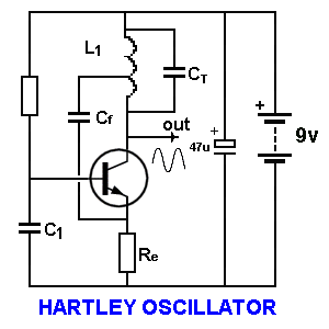
The operation of the circuit is the same as a Colpitts Oscillator. The Colpitts Oscillator is the easiest to build because a tapped coil in the Hartley Oscillator needs 3 wires and is very messy to wind and solder to a PC board. A Hartley Oscillator has no advantages over a Colpitts Oscillator.
For an oscillator to produce a waveform, it must have a FREQUENCY DETERMINING NETWORK.
In the two oscillators above, the FREQUENCY DETERMINING NETWORK is the TANK CIRCUIT.
The feedback capacitor does not have any effect on the frequency (only a small effect when say it is doubled or halved).
In the Phase Shift Oscillator, the feedback components DETERMINE THE FREQUENCY.
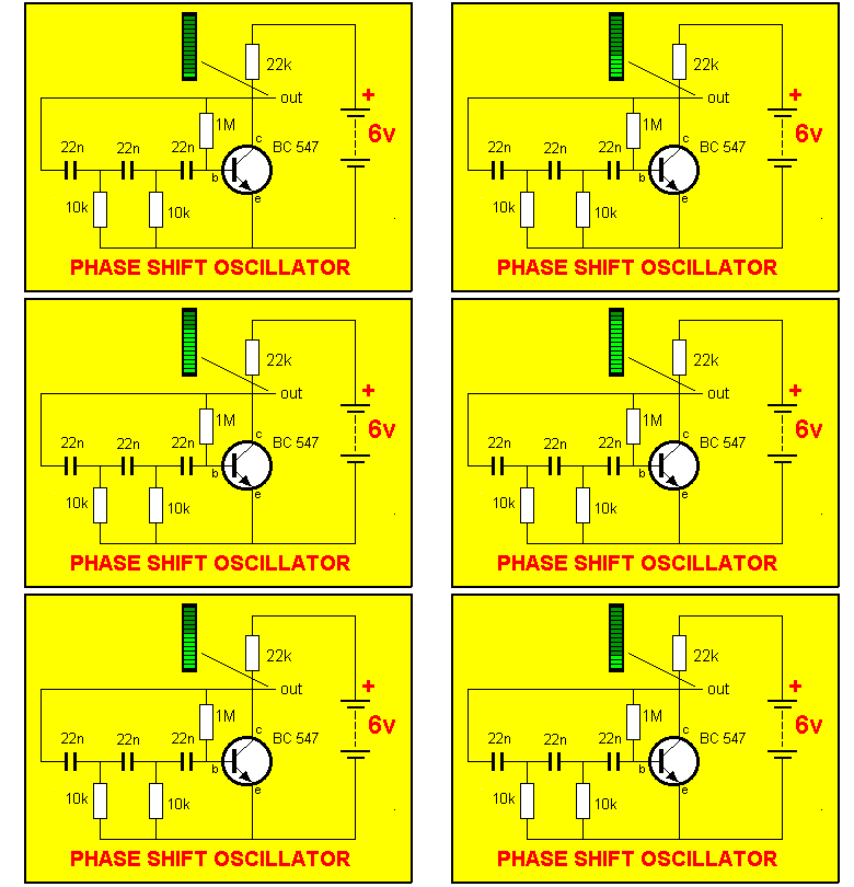
Phase Shift Oscillator The Phase Shift Oscillator uses the charging of a capacitor via a resistor to produce a time delay. In this circuit, there are three time-delay sections made up of a 22n and 10k resistor, with the third delay using the base-emitter junction as the resistor. The operation of the circuit is very complex, so we will simplify the description.
The output is a smooth rising-and-falling waveform - a SINEWAVE.
When the power is applied to the circuit the transistor will immediately turn on FULLY as the three 22n capacitors will acts as “short-circuits” and current will pass to the base and the collector voltage will fall to a very LOW level.
The capacitors will gradually charge via the 10k resistors and the voltage across the second 10k resistor will drop (due to the charging current into the middle 22n gradually reducing) and the voltage on the left lead of the 3rd 22n will drop. This will reduce the voltage on the right lead of the 22n and turn the transistor OFF. The first two 22n’s will start to charge but the voltage across the 2nd 10k will be very small and the 3rd 22n will start to charge via the 1M resistor.
The charging of the first 22n is much faster than the charging of the third 22n and the voltage on the output rises to almost rail voltage. This allows the 3rd 22n to charge at a faster rate and just when the collector voltage reaches a maximum, the base voltage reaches 0.6v and the transistor starts to turn ON.
This lowers the collector voltage but the transistor still keeps turning ON via the 1M and the three 22n start to charge. This action increases the “turn-ON” of the transistor and it continues to turn-ON until the voltage on the collector reaches a very LOW level.
The circuit works completely differently to anything described in any Text Book. The transistor operates on a rising and falling CURRENT (increasing and decreasing current) into the base. That’s why no-one has described it before.
The third 22n continues to charge and the “turn-ON” current for the transistor reduces and it starts to turn OFF a slight amount. The second 10k continues to charge the middle 22n and the voltage across the 10k reduces. This pulls the left lead of the third 22n towards the 0v rail and the right lead follows. This action turns OFF the transistor and the collector voltage rises.
FEEDBACK in an OSCILLATOR
Only a small portion of the OUTPUT SIGNAL in an oscillator is fed back to a previous part of the circuit. It only needs a small amount to keep the oscillator working.
This is generally done with a capacitor. A capacitor will deliver a signal while preventing the voltage on the output from being passed to the input of the oscillator - it only passes the signal. The voltage on the output is much higher than the voltage on the input and these two values need to be separated and only the signal (the waveform) passed from the output to the input.
A capacitor will ATTENUATE (reduce the amplitude) of the output signal and only deliver a “miniature version.” It does this because the capacitor charges during the time when the signal is rising and the voltage developed across the capacitor is subtracted from the signal being delivered. That’s why the value of the capacitor is important. By selecting a smaller value, a smaller waveform is passed to the small-signal section of the circuit.
The “signal” is a rising and falling voltage and this voltage must ASSIST the rising and falling voltage on the input. This signal is called a POSITIVE FEEDBACK signal.
A waveform is a signal or a line drawn on graph paper or a “trace” on a Cathode Ray Oscilloscope that generally starts at the 0v rail and rises to a peak. It then decreases to the 0v rail. It may also pass through the 0v rail and travel in the negative direction to the same negative amplitude of the peak. It then travels to the 0v rail to complete ONE CYCLE.
A complete cycle is drawn on GRAPH PAPER with 0° at the beginning of the cycle and 360° at the end, so you can work out the various parts of the waveform for positive or negative feedback. This allows us to talk about what is happening at 90° or 180° or at any other part of the graph.
It doesn’t matter if the waveform is a sine-wave, square-wave or triangular, it can be drawn on a grid with the start of the wave at 0° and the end at 360°.
To work out if the output waveform will deliver a Positive or Negative feedback signal, a second graph needs to be drawn. The second graph is drawn below the first graph and a ruler is placed vertically to align the two graphs. You can then see what is happening at one point on the top graph and compare it to the signal on the lower graph.
These graphs will need to come from the traces on a dual-race Cathode Ray Oscilloscope.
Make the top graph the “small-signal” graph and lower graph from the output of the oscillator.
Move a perpendicular ruler across the graph and watch the rise of the small-signal. If the “small-signal” is rising and the output signal is rising, the result will be POSITIVE FEEDBACK.
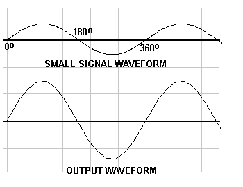
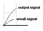
The output signal has a high amplitude and is above the “small-signal” will “pull-up” (assist - increase) the small signal and thus keep the oscillator working
IN PHASE
On the graph you can see the signal is rising from the 0v rail at 0°. The graph continues and at 360° the signal will rise again from the 0v rail to start the next cycle.
This means the signal at 0° and 360° are doing the SAME THING - it is rising. These two parts of the graph are IN PHASE. In other words both lines on the graph are identical (in the way they are moving UP) - one line can be placed on top of the other and they are the same.
OUT OF PHASE
The signal at 0° is rising and the signal at 180° is falling.
This is called OUT OF PHASE - the two lines on the graph are not going in the same “up” direction.
There are two types of feedback signals in electronics. POSITIVE and NEGATIVE.
If the signal strengthens the signal in the “small-signal” section, it is called POSITIVE FEEDBACK and is IN PHASE. This means the two signals are rising at the same time and on the graph they are 360° apart, but in reality they are rising AT THE SAME TIME.
If the output signal REDUCES the waveform of the small-signal, it is called NEGATIVE FEEDBACK and the signals are NOT IN PHASE. On the graph they are 180° apart but in real-time one signal is rising and the other is falling AT THE SAME TIME.
A POSITIVE FEEDBACK signal ASSISTS the small-signal.
A NEGATIVE FEEDBACK signal reduces the amplitude of the small-signal.
Another name for POSITIVE FEEDBACK is BOOTSTRAPPING. A large percentage of the output is intentionally passed back to the front-end to assist the incoming signal. The result is a very large output. See Stereo VU Meter project for a Bootstrap Circuit. The same circuit is also here. Another circuit showing the effect of Positive Feedback is the Clap Switch. The effect can also be called REGENERATION, where a small change is passed to an output then back to the input to create a larger change his circulated around the two stages until the are both turned ON fully.
Positive Feedback and Bootstrapping can have a very large effect on the incoming signal and increase the output to a point where clipping or distortion occurs as shown in the Clap Switch circuit. The two components creating the Positive Feedback are the 100u and 100k in series.
Another name for NEGATIVE FEEDBACK is ERROR SIGNAL or ERROR FEEDBACK. If the output contains distortion or spikes, these parts of the waveform will not be present in the small-signal waveform. By sending the output back to the small-signal section and combining the two waveforms, the Negative Feedback signal will have an effect on reducing those parts of the waveform that are different. The peaks or bumps will be reduced and these are the parts of the waveform called “distortion.”
PHASE REVERSAL
A rising signal on the base of a common emitter transistor will produce a falling signal on the collector. This has been covered in the section: The Transistor.
This is called PHASE REVERSAL or SIGNAL REVERSAL. In other words the signal is OUT OF PHASE by 180°. This will produce a NEGATIVE FEEDBACK signal.
To produce a POSITIVE FEEDBACK signal, the signal must be at 0° and 360° on the graph so they are IN PHASE.
How do you get a signal that is 360° out-of-phase?Here is the answer:A second common emitter stage will produce 180° phase-shift, making a total of 360° phase-shift to produce a POSITIVE FEEDBACK signal.
In other words, two stages of reversal is the same as non-reversal. 360° phase-shift is the same as 0° phase-shift.
PHASE-SHIFT is **NOT DELAY. Phase-shifting simply means the incoming signal has a slightly higher amplitude and is rising at the same rate to provide Positive Feedback. Or the incoming signal may traveling in the opposite direction to provide Negative Feedback. Negative feedback simply means the incoming signal is “pushing down” on the small signal and reducing its amplitude. The incoming signal will have more effect on the peaks and that’s how distortion is reduced or removed.
When looking at the waveforms for FEEDBACK, we are not interested in FREQUENCY or PERIOD. We are just looking at the timing of one waveform and comparing it to another to achieve Positive or Negative feedback.
“Timing” means the relative position of one wave on the graph, then looking at the other wave to see if it ASSISTING or CANCELING the “small-signal.” We have already motioned above, how to work out how the incoming waveform is affecting the “small-signal.”
That’s why we don’t have a TIME SCALE on the graph.
The waveforms we are studying are called PERIODIC WAVEFORMS. In other words they repeat. The waveform can be any shape or size, as long as the next cycle is identical to the previous.
An example of a non-periodic waveform is speech. Each cycle is slightly different to the previous. However a tone or whistle is periodic because each wave is very nearly identical to the previous.
The easiest way to create a Positive or Negative feedback signal is to experiment with an actual circuit.
The value of the capacitor is VERY CRITICAL. It may be 10p or as high as 10u. Sometimes a resistor can be added in series with the capacitor. This will alter the “timing” by delaying the effect of the capacitor and since the combination of the two values will produce an enormous number of possibilities.
We explained above, the capacitor will pass nearly all the amplitude of the output waveform to the small-signal section or only a small percentage of the amplitude, depending on its value.
If it is small, it will get charged during the transfer and most of the amplitude will be lost (ATTENUATED). The actual percentage transferred will also depend on the frequency as the capacitor will not be able to charge very much when the frequency is very high. At low frequency, the same-value capacitor will charge to a higher voltage because it has more time to charge.
To see exactly what is happening, you need a need a piece of test equipment.
That’s why we use a CRO (Cathode Ray Oscilloscope). It has a screen and you can watch what happens when you change the value of a component.
Sometimes, a slight change in the value of a component will alter the operation of the circuit considerably and that’s why you cannot predict what will happen or use any form of simulation software. You MUST build a circuit and test it.
In place of a coil and capacitor to create the frequency of oscillation, we can use a CRYSTAL.
A crystal resonates (produces a vibration) when a voltage is applied across it and this changes its resistance. The current though the crystal is detected by a transistor and is amplified. There is no feedback in this circuit because the crystal operates as soon as a voltage is applied.
This oscillator is never mentioned in any text books but is one of the most-used oscillators.
It is used in TV sets that have a Cathode-ray Tube, CRO’s (Cathode Ray Oscilloscope - test equipment), Monitors using a CRT, boost converters, High-Voltage generators, Joule Thief Circuits and many more.
It is a circuit using the amazing fact that if you instantly turn off the current (voltage) to a coil (transformer, relay, inductor or choke), it will produce a very high voltage (in the reverse direction).
This voltage is called FLYBACK VOLTAGE and can be up to 500 times higher (or more) than the supply voltage.
The coil must be connected to a circuit to via a transistor. A feedback waveform is taken from the coil to turn the transistor OFF very quickly to produce the FLYBACK VOLTAGE and the circuit can be made to oscillate at a frequency from 20kHz to more than 100kHz.
This is one of the most important oscillators to study because it is used is many common devices.
Even though it uses only 4 components, its operation is very complex and the inductance of the coil (transformer) is the main component to determine the frequency as well as the capacitor on the base and the base-bias resistor.
Here are 4 projects that used the Flyback Oscillator to produce a voltage higher than the supply.
1. BIKE FLASHER
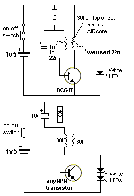
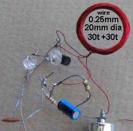
This circuit uses an air-cored transformer to show that a metal core is not needed to produce the “flyback effect.”
The first circuit illuminates the LED with constant brightness. A white LED requires 3.6v to illuminate and the voltage of the 1.5v cell is increased by the circuit to illuminate the LED. The two 30 turn coils can be separated to see the effect of separation and metal items can be inserted in the centre to see the effect they produce.
This is an ideal circuit for experimentation.
2. TRANSISTOR and LED TESTER
The project in .pdf
<!-- TODO FIXME COLIN: can you make the above PDF a page on the site?


3. ZENER TESTER
The project in html format.


4. COMPACT FLUORESCENT LAMP DRIVER


OUTPUT WAVEFORM
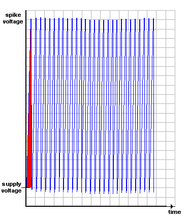
The output waveform from a flyback transformer consists of very high voltage spikes very similar to the graph below. The area under the graph (shown in red on the first cycle) represents energy and the spikes are very narrow and very tall. This represents a very high voltage and the component connected to the output of the transformer will see this high voltage and start to “breakdown.”
This is called a non-destructive breakdown. (mainly because the current is not high enough to produce destruction).
In other words, the component will start to take current when a certain voltage is reached and the high-voltage spike will stop at this level and during the remainder of the spike, current will be passed to the device.
In the case of the Zener Tester, the voltage will rise to the characteristic voltage of the zener under test and then the energy of the spike will charge the 1u. Placing a voltmeter across the zener will let you know the zener voltage.
In the case of a LED, the voltage across the LED will reach a maximum of 3.6v for a single white LED and the voltage will not rise further.
In the case of a CFL, the 600v spike will “strike” the lamp (ionize the gas) and then the gas will produce a voltage across the leads with a characteristic value of about 100v and the remainder of the spike will deliver current to produce illumination.
It is easy to see the operation of the CFL circuit because the CFL tube is not-polarised and will operate “either-way-around.”
The transformer in a fly-back circuit does not operate on a “turns-ratio” basis and the voltage produced by the secondary cannot be worked out by any formula.
The primary is 50 turns and the output is 500 turns. This is a 1:10 turns-ratio and would normally produce an output of 120v if the circuit was a sine-wave. But with a fly-back circuit the output is due to the rapid collapse of the magnetic flux and will be more than 500v.
The output of the circuit produces a very high voltage when the flux collapses and this voltage is a spike with the positive on (say) the top lead. There is no high voltage in the reverse direction.
The same theory applies to the other circuits but the output voltage is less due to the smaller number of turns on the winding.
This time the output is taken from the primary because the transistor is effectively “removed from the circuit” during part of the cycle when it is turned off and the winding is only connected to an output device.
The bottom lead of the winding becomes positive and this voltage adds to the supply voltage.
You can see the output component (LED or zener) is connected to this voltage and the other end of the LED is connected to 0v.
Thus it gets the voltage produced by the winding PLUS the battery voltage.
TURNS
How is the number of turns on the transformer determined?
There are no formulas for this.
The load must be connected and illuminating brightly for the transformer to take the least current. If the load is removed, the core will become saturated and the current will increase considerably.
So, where do you start? You really have to look at previous designs because there is no starting-point.
Wind 60 turns on the primary and make a tapping at 40 and 50 turns.
Wind 600 turns on the secondary and make a tapping at 300 and 400 turns.
This will give you 6 experiments to work out the best brightness and the lowest current.
You can also connect the output to an 18 watt (20 watt fluorescent tube) and the whole room will be filled with illumination as the tube is 3 times more efficient than a CFL.
THE POSITIVE FEEDBACK OSCILLATOR
Fig 41 is a circuit that will illuminate a LED and fig 42 will flash a LED. The only difference is the addition of the 10u electrolytic. The circuit is actually a very high-gain amplifier and this is shown by the fact that a 330k resistor is the input component supplying the input current and the 2 transistors amplify the current through this resistor (2 microamps) and provide enough current to flash a LED very brightly. The very brief flash is due to a term called POSITIVE FEEDBACK - it changes the performance of circuit completely. It makes the circuit OSCILLATE. Negative feedback “kills” a circuits performance - positive feedback makes it oscillate. It increases the signal so much that the circuit becomes unstable. This is called oscillation.
The 2 transistors have a lot of amplification and they will illuminate the LED, but the 10u electrolytic actually INCREASES the amplification considerably and this makes the LED flash even brighter. But it can only do this for a short period of time (when it is charging). When it gets charged, it can no longer provide this “boost” and the circuit will “move in the opposite direction” as we have explained below.

Fig 41.
Fig 41 shows a circuit using an NPN and PNP connected via a 1k resistor and turned ON via a 330k base resistor.
The LED will illuminate.
There is nothing magic about this circuit. It is simply a HIGH-GAIN, DC-AMPLIFIER using two transistors.
The values of current are only approximate and show how each section allows an increasing amount of current to flow.
A current of 100mA is too high for a LED and it will be damaged. This circuit demonstrates the possible current-flow. If this current flows for a very short period of time, the LED will not be damaged. Fig 42 shows how the circuit is converted to an oscillator or “flasher.”

Fig 42.
Fig 42. When we connect a capacitor as shown, an amazing thing happens. The high-gain amplifier turns into an OSCILLATOR.
When the voltage on point “X” is rising, the voltage on point “Y” is rising TOO. But point “Y” rises much higher than point “X.”
This means that if we DIRECTLY join points X and Y, the voltage-rise from point Y will push point X higher and turn the circuit ON more. This will continue until the circuit is fully turned ON and the two transistors are SATURATED.**This effect is called POSITIVE FEEDBACK and the circuit will get turned ON until it cannot turn on any more. But we haven’t joined points “X” and “Y” DIRECTLY (we have used a capacitor) so we have to start again and explain how the circuit works.
When the power is applied, the 10u gradually charges and allows a voltage to develop on the base of the NPN transistor. When the voltage reaches 0.6v, the transistor turns ON and this turns on the PNP transistor.
The voltage on the collector of the PNP transistor increases and this raises the right side of the 10u electrolytic and it firstly pushes its charge into the base of the NPN transistor. Then the 330k takes over then it continues to charge in the opposite direction via the base-emitter junction of the NPN transistor. This causes the two transistors to turn ON more. This keeps happening until both transistors cannot turn ON any more and the 10u keeps charging. But as it continues to charge, the charging current eventually drops slightly and this turns off the first transistor slightly. This gets passed to the PNP transistor and it also turns off slightly. This instantly lowers both leads of the 10u and both transistors turn OFF.
The 10u is partially charged and it gets discharged over a long period of time by the 330k resistor and when it starts to charge in the opposite direction, the base of the first transistor sees 0.6v and the cycle starts again.
The end result is a very brief flash and a very long pause (while the capacitor starts to charge again).
As you can see, there is very little difference between a high-gain DC amplifier and the oscillator circuit just described.
That’s why you have to be very careful when looking at a circuit, to make sure you are identifying it correctly.
An oscillator is sometimes represented by a “block” with an output. The output-line means a frequency is output from the oscillator.
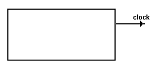
Sometimes the shape of the oscillator waveform is identified: In the first block the oscillator is a square wave with a mark-space ratio of 50:50
The second block produces a “pulse.”

The clock line entering a chip is called the CLOCK LINE. This means the components inside the block cannot produce a waveform. They my be just counting registers or divider-stages.
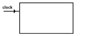
The word “clock” on a chip (Integrated Circuit) means a square wave (or a pulse as shown above) must be supplied to the chip. The chip does not have an internal oscillator components:
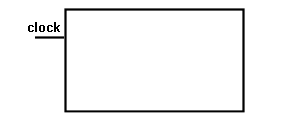
If the chip has internal oscillator components (such as an amplifier in the form of an Op-Amp) it will require external timing components (resistors and capacitors).
This will be shown as:
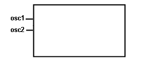
The operation of a chip counting via an incoming cock can be stopped (halted - frozen - inhibited) by an input called the INHIBIT LINE. This stops the chip counting when the line is HIGH and the chip continues to count when the line goes LOW: The clock pulses enter the chip but do not increment the counting stages when Inhibit is HIGH.

A CLOCK LINE can control (increment) more than one chip at the same time:

Each chip can have an inhibit line so that it can be started and stopped individually:

All the above are digital lines. The clock line is digital and the inhibit line is digital. In other words, the lines rise and fall very quickly.
The output of an oscillator can be ANALOGUE - a Sinewave is analogue:
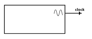
You should not deliver an analogue clock signal to a digital chip. Digital chips do not like analogue signals.
A digital chip requires the rise and fall to be very fast as the chip changes from detecting a LOW to detecting a HIGH during the middle of the excursion (about 50% of rail voltage) and if the signal is slow, the chip will begin to oscillate internally and produce many clock pulses, for each incoming cycle.
Some chips have a Schmitt Trigger feature on the input to prevent this problem.
OUTPUT AMPLITUDE of an OSCILLATOR
The amplitude of the output of an oscillator must be viewed on a CRO to determine if it is the correct height. It will also give some idea of the frequency, but a frequency-meter is needed for an accurate read-out.
Some oscillators produce a rail-to-rail waveform. This is the largest amplitude possible for the supply voltage you are using - such as 5v or 9v or 12v.
But if the biasing is not correct (biasing is the value of the base resistor emitter resistor and load resistor), the waveform will be small or LARGER than required. If it is too large, it will touch the supply rail and the top of the wave will be cut-off and have a “flat-top.”
There is one other important point that is never mentioned in any text book.
Some oscillators are high-impedance and some are low-impedance. A low-impedance oscillator (circuit) will deliver a current on its output line and the amplitude will not reduce.
A high-impedance oscillator (circuit) does not have any “driving power” and needs to be connected to a buffer stage.
Every time you connect the output of an oscillator to a “counting chip” or to another stage, some of the oscillator’s energy is delivered and this will reduce the amplitude of the wave.
To find out if the oscillator is being overloaded, you can connect a resistor between the output and rail voltage. Then connect a resistor between output and 0v. Reduce the value of the resistor until the oscillator ceases to oscillate.
This will give you some idea of the “driving power.”
THE WAVEFORM of an OSCILLATOR
All oscillators produce a WAVE - also called a WAVEFORM.
The waveform represent the output VOLTAGE.
Generally one cycle is drawn, starting from the 0v rail and returning to 0v rail.
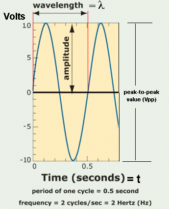
The WAVELENGTH is the distance between the start of a cycle and the end of the cycle. This is shown on a graph via a TIME scale and in the graph above, the cycle takes 0.5 seconds. This produces a frequency of 2 cycles per second and is 2Hertz.
The AMPLITUDE of the signal is the distance from the 0v rail to the maximum height. On the graph above this is shown as 10v.
Peak-to-Peak
This is the distance between the minimum and maximum value. On the graph above, this is 20v.
Here are some CRO waveforms:
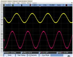
Two sine-waves. The red wave has a higher amplitude and frequency.
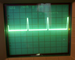
A pulse or trigger waveform.
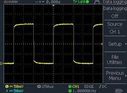
A square wave with sight rounding of the edges.
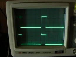
A square wave with slight “overshoot” on the lower trace.

10kHz sinewave - 100Hz square-wave
THE MAGNETIC CIRCUIT
All of the oscillators using an inductor use a coil or transformer that is wound on a core made of ferrite.
Ferrite is similar to a powdered iron material in which the iron particles are very small to prevent the core heating up due to currents flowing in the material.
These currents are called “Eddy Currents.”
But the topic we want to cover is the concept of a MAGNETIC CIRCUIT. It is the path where the “magnetism flows.” In the first diagram the magnetism flows through the rod and is “lost” out the end of the rod. In the second diagram the magnetism flows through the core and through a gap called an air-gap. In the third diagram there is no air gap.
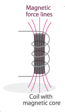
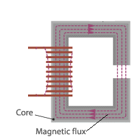
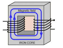
The third diagram is called a transformer because it has a secondary winding.
If you connect the transformer to the AC mains, the first winding on the core is called the primary and when you wind 5 turns for each volt of the mains voltage and connect the transformer, the primary winding will take very little current because the magnetic flux produced in the core will produce a back-voltage that is almost equal to the incoming voltage.
The magnetic flux is only capable of producing 0.2v per turn.
If you reduce the number of turns to 4, the magnetic flux will only produce a back-voltage of 0.8v and this will allow a forward voltage to enter the primary winding. This will cause a current to flow due to the resistance of the primary winding.
This means the primary winding will get hot, even though the transformer is not providing a current to a load.
In the second diagram, an air gap is introduced. A lot of the magnetic field is lost in the air gap and the magnetic field cannot produce 0.2v for each turn. This will allow a forward voltage to enter the primary winding and a current to flow due to the resistance of the primary winding.
If we connect a load to the second diagram, some of the magnetic flux will cut the secondary turns and create a current (and voltage) for the load. This will cause a current to flow in the primary made up of current for the air gap and current for the load.
To prevent current flowing in the primary, the voltage must be reduced.
In the first diagram, only a very small voltage can be applied or the turns per volt must be a high number so the core is not saturated.
The storage of magnetic energy in the core material is between 100 and 1,000 times greater than air.
Now we come to the second part of the investigation.
If we take the third diagram and connect it to the AC supply, almost no current will flow in the primary.
If we introduce a small air-gap, a small current will flow in the primary. If we increase the width of the air gap, more current will flow.
If we take the original third diagram and load the output to a maximum, current will flow in the primary. If we introduce a small air gap, no additional current will flow because the flux in the magnetic circuit will provide a feedback voltage at the peaks of the AC waveform. But if the load is reduced, there is not enough magnetic flux in the core to produce a feedback voltage because a lot of the flux has been lost in the air-gap.
This means a “open circuit” magnetic path (such as in the first diagram) will work successfully if all the flux is absorbed by the secondary, either during the energising part of the cycle or removed during the remainder of the cycle, so the magnetic dipoles can be energised again. They are energised by being turned in one direction.
METAL DETECTOR OSCILLATORS
All the oscillators we have covered above are designed to produce a STABLE OUTPUT.
In general we don’t want an oscillator to drift - change frequency - but there is a range of oscillators that are VERY UNSTABLE.
The correct term for these oscillators is very SENSITIVE
These oscillators have the coil exposed and the turns have a very large diameter.
This type of oscillator is used to detect the presence of a metal object. The metal will alter the inductance of the coil by absorbing some of the magnetic flux and increase or decrease the frequency of the circuit, depending on the type of metal.
There are two types of metal - as far as magnetism is concerned. Magnetic and non-magnetic.
But when an oscillating magnetic field is present, another feature is present.
All metals that conduct electricity will produce eddy currents when exposed to an oscillating magnetic field and this will absorb some of the magnetic flux.
This will increase the inductance of the coil and reduce the frequency.
Most of the oscillator circuits are Colpitts and can consist of 5 to more than 15 components.
The whole idea of the circuit is to make it stable when “sitting around” but allow the slightest magnetic influence to change the frequency.
This is called the SENSITIVITY of the circuit and we will be providing a number of circuits for you to test and compare their sensitivity.
These circuits operate between 100kHz and 500kHz and to detect when they shift by as little as 1Hz, we use a stable reference oscillator. The oscillator is an AM radio. It has an inbuilt 455kHz oscillator and when placed near a Metal Detecting Oscillator, it picks up the signal, (just like a radio station) and produces a whistle. This whistle represents the difference in frequency of the two oscillators.
It is called a BEAT-FREQUENCY or Difference Frequency.
By tuning across the band you will get a lowering in frequency until the whistle stops. At this point the two oscillators are the same frequency or one is a multiple of the other and the difference produces a zero- frequency beat. If a coin is brought near the detecting coil, the change in frequency will be heard.
Even though this arrangement is very simple, it is equal to all the BFO (Beat Frequency Oscillator) Gold detectors on the market.
The circuits inside the detectors have both the single transistor oscillator and the radio components, in one circuit.
This means all the radio circuit can be neglected and we have only have to concentrate on the oscillator, to find the most sensitive circuit.
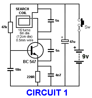
The circuit is a Colpitts Oscillator and is placed near an AM radio to produce a whistle.
The circuit operates at about 500kHz.
The radio is tuned so the whistle is reduced to zero. When a metal object is placed near the coil, the frequency of the transmitter is reduced and a whistle is heard in the radio.
Compare this circuit will the other circuits to determine the most sensitive.
Note: 4n7 between collector and emitter produced a better signal - easier to find on AM radio.
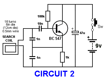
This circuit is a good performer. Current 4mA. Easy to find signal on AM radio. The circuit operates at about 1MHz and the beat-frequency can be found on the dial at 1,000kHz.
In this circuit the coil is not driven directly but receives a very small amount of energy from the feedback provided by the signal on the emitter of the transistor.
The coil and the two 1n capacitors (in series) produce a TUNED CIRCUIT and will produce natural oscillations. The transistor sees this and produces the same waveform on the emitter but with a greater amount of “strength.”
This “strength” is not needed by the Tank Circuit but it needs a signal and the signal from the emitter is sufficient to maintain oscillation.
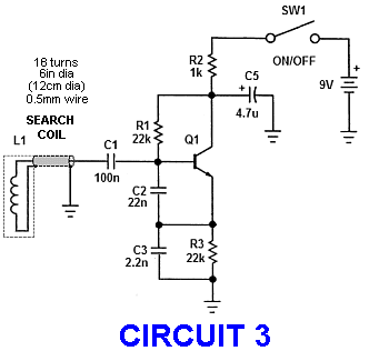
By keeping the size of the search coil nearly the same in all circuits, we can determine if the arrangement of the components improves the sensitivity.
Circuits 2 and 3 are SHUNT-FED Colpitts Oscillators.
In a Shunt-fed oscillator, DC is not passed through the Tank or Oscillator section.
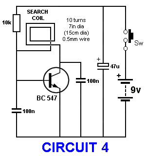
This is a very simple circuit produced by a reader. See if it works.
Circuit does not work with 10k. Reduce 10k to 3k3 and circuit keeps changing frequency. Very hard to find on AM radio.
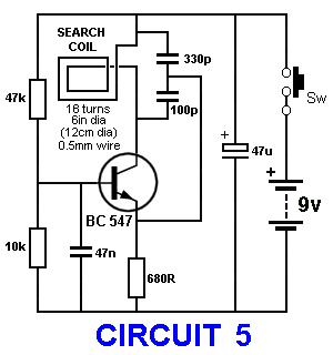
This circuit is the same as circuit 1 but the TUNING CAPACITOR across the coil is tapped and the tapping (feedback) is passed to the emitter.
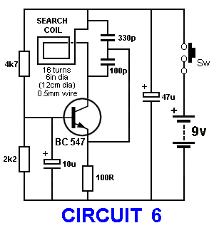
This circuit is the same as circuit 5 but the emitter resistor is reduced and the transistor takes more current. See if this improves the sensitivity.
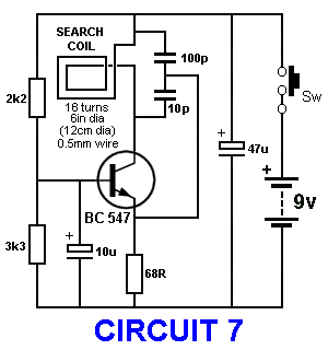
Every component in this circuit is the wrong value.
Build the circuit and see if it works.
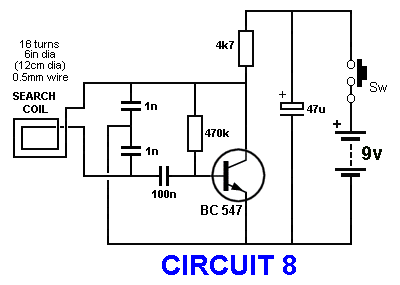
This circuit is the best performer. Current 2mA. Easy to find the signal on AM radio. The circuit operates at about 1MHz and the beat-frequency can be found on the dial at 1,000kHz.
The circuit is very similar to #2 but this time the feedback signal from the collector has a larger amplitude and the voltage across the coil is about 15v p-p. This produces a very clean and clear signal on an AM radio and is the best performer of all the circuits.
The Tank Circuit operates in a very unusual way.
The tapping (between the two capacitors) is connected to 0v and does not move.
When the magnetic flux in the coil collapses, it charges both 1n capacitors in series and although it does not charge both equally, the bottom terminal of the coil drops downwards easily because the base-emitter junction of the transistor is seeing a reverse-voltage and does not offer any opposition.
This turns the transistor OFF and the top 1n starts to charge via the 4k7 resistor. The top terminal of the coil rises due to the charging of the top 1n and as the voltage produced by the coil reduces, the voltage on both ends of the 100n starts to rise and turn ON the transistor.
The voltage across the base-emitter junction cannot rise above 0.7v, so the transistor turning ON will remove the voltage across the top 1n
Changing the 100n “pick-off” to 10n makes no difference so the value of this capacitor is not important. It simply connects the tank circuit to the transistor and does not affect the timing of the circuit.
METAL DETECTOR OSCILLATORS - CONCLUSION
The best circuit is #8 where the Tank Circuit (the self-oscillating circuit - the coil and capacitors) will produce a good waveform (large amplitude) that is easy to pick-up on an AM radio at about 1,000kHz.
Don’t forget, this circuit is a special type of oscillator that is stable in operation but is easily “upset” by the change inductance of the coil.
This means the Tank Circuit has to be lightly loaded and although it is connected to the base via a 100n capacitor, the transistor is providing a feedback signal that is compensating for the losses delivered to the base.
The emitter waveform was measured on a CRO as 15v p-p for 9v supply. The transistor is a common-emitter amplifier and the circuit is a SHUNT-FED Colpitts Oscillator because no DC is passed through the Tank (oscillator) section.
These 8 circuits are a perfect example for an experiment to show you cannot predict how a circuit will work and which circuit will perform the best.
No simulation-software package will show the enormous difference between the circuits. That’s why you have to build EVERYTHING and OBSERVE the results yourself.
The secret to getting a TANK CIRCUIT to produce a good sinewave is shown in circuit 8.
The reason why a Tank Circuit will produce a voltage up to twice rail-voltage is due to the fact that the inductor produces a voltage in the reverse direction when it collapses.
Quick Links
Legal Stuff
Social Media


